
A Miniaturized Photoelectric Oscillator Based on SIP Packaging Technology

A photoelectric oscillator and technology, applied in the direction of electric solid-state devices, circuits, electrical components, etc., can solve the problems of inability to realize the isolation of optical signals and electrical signals, difficulty in generalization, and low yield rate, so as to ensure normal and stable work , Improve packaging density, good microwave performance effect

Active Publication Date: 2022-07-29
SHANGHAI RADIO EQUIP RES INST
View PDF12 Cites 0 Cited by
  • Summary
  • Abstract
  • Description
  • Claims
  • Application Information

AI Technical Summary

Problems solved by technology

Compared with the present invention, it cannot realize the isolation of optical signal and electrical signal, and does not form a package, the yield rate is low, the heat dissipation is poor, and it is difficult to achieve generalization

Method used


Image

  • A Miniaturized Photoelectric Oscillator Based on SIP Packaging Technology
  • A Miniaturized Photoelectric Oscillator Based on SIP Packaging Technology
  • A Miniaturized Photoelectric Oscillator Based on SIP Packaging Technology

Examples


Embodiment Construction

[0029] The preferred embodiments of the present invention will be described below with reference to the accompanying drawings.

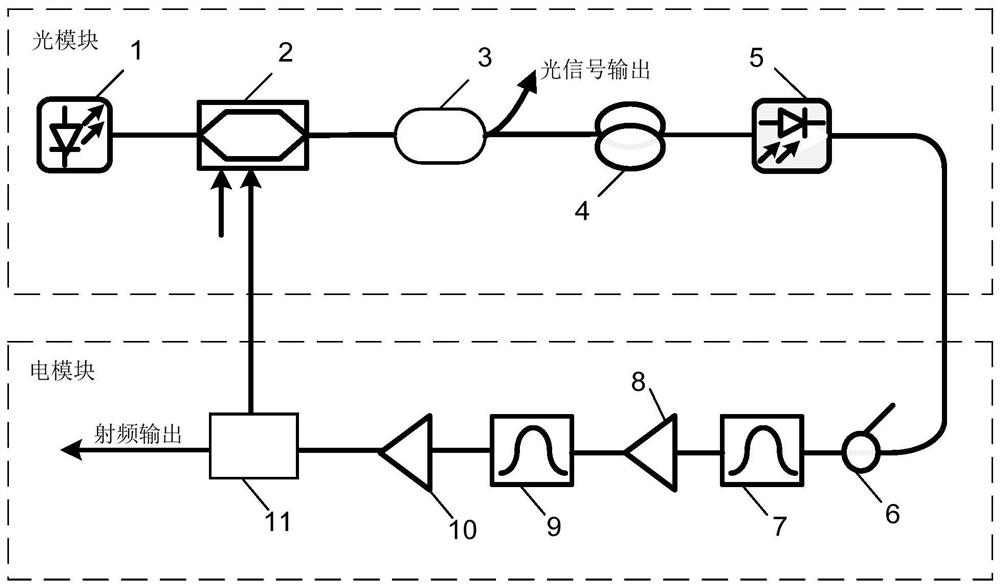
[0030] The present invention provides a photoelectric oscillator system based on SIP package (system-in-package) integration technology. like figure 1 As shown, the system is provided with an optical module 15 of an optoelectronic oscillator and an electrical module 16 of an optoelectronic oscillator. The optical module 15 includes: a YAG laser 1 (yttrium aluminum garnet laser), a Mach-Zehnder electro-optical modulator 2 (Mach-Zehnder electro-optical modulator), an optical coupler 3, an optical delay unit 4, and a photodetector 5. The electrical module 16 includes: a single-pole single-throw switch 6 , a first ESC filter 7 , a first low-noise amplifier 8 , a second ESC filter 9 , a second low-noise amplifier 10 , and an electrical coupler 11 . The radio frequency insulator 21 ( image 3 ) to realize the signal interconnection between the optical m...


PUM


Abstract

The invention discloses a miniaturized photoelectric oscillator chip based on SIP packaging technology, comprising a photoelectric oscillator optical module, a photoelectric oscillator electrical module and a metal ceramic shell for packaging; the components of the optical module are sintered on a gold-plated surface by a gasket. On the bottom surface of the housing, the components of the electrical module are sintered on the bottom surface of the gold-plated housing by digging holes in the microstrip plate, and transmit signals through the microstrip plate; the optoelectronic oscillator chip presents modular isolation, and the optical module and the electrical module are isolated by a metal partition , and the light-absorbing material and the wave-absorbing material are respectively coated on the outside of the partition. Signals such as power supply and output of the optoelectronic oscillator chip are transmitted through the pins of the Ceramic Quad Flat Package (CQFP). The invention utilizes the SIP packaging technology to realize the chip-based three-dimensional integration of the low-phase noise photoelectric oscillator, realizes integrated, light and small, tunable, electromagnetic compatibility design, greatly reduces the volume and weight of the photoelectric oscillator system, and satisfies the future radar frequency synthesis system. Modularization, high reliability, miniaturization and other development needs.

Description

technical field [0001] The invention relates to the field of radio frequency transceiver, and specifically designs a miniaturized photoelectric oscillator based on SIP packaging technology, which can be applied to the fields of communication systems, radar, space detection and the like. Background technique [0002] Oscillators play an important role in radar, navigation and guidance, communication systems, instrument measurement and other fields, and directly affect the performance of electronic systems. As a new type of microwave signal source combining optical circuit and circuit, photoelectric oscillator can generate optical and electrical signal outputs with high quality factor, high spectral purity and low phase noise. It is expected to be used as a high-quality microwave signal source for electronic systems in the future. . [0003] Existing photoelectric oscillators generally use multiple modular devices to connect, and have not yet been able to achieve miniaturized...

Claims


Application Information

Patent Timeline
Patent Type & Authority Patents(China)
IPC IPC(8): H01L23/06H01L23/373H01L23/552H01L25/16
CPCH01L23/06H01L23/373H01L23/552H01L25/16
Inventor 潘超群苏坪徐晟丁勇郭培培周王伟刘永杰
Owner SHANGHAI RADIO EQUIP RES INST
Learn More