
Silicon integrated BTO film and preparation method thereof
A thin film and transition layer technology, applied in the field of silicon integrated BTO thin film and its preparation, can solve problems such as poor performance of BTO thin film, and achieve the effects of easy control, large coating area and high ferroelectric performance
- Summary
- Abstract
- Description
- Claims
- Application Information
AI Technical Summary
Problems solved by technology
Method used
Image

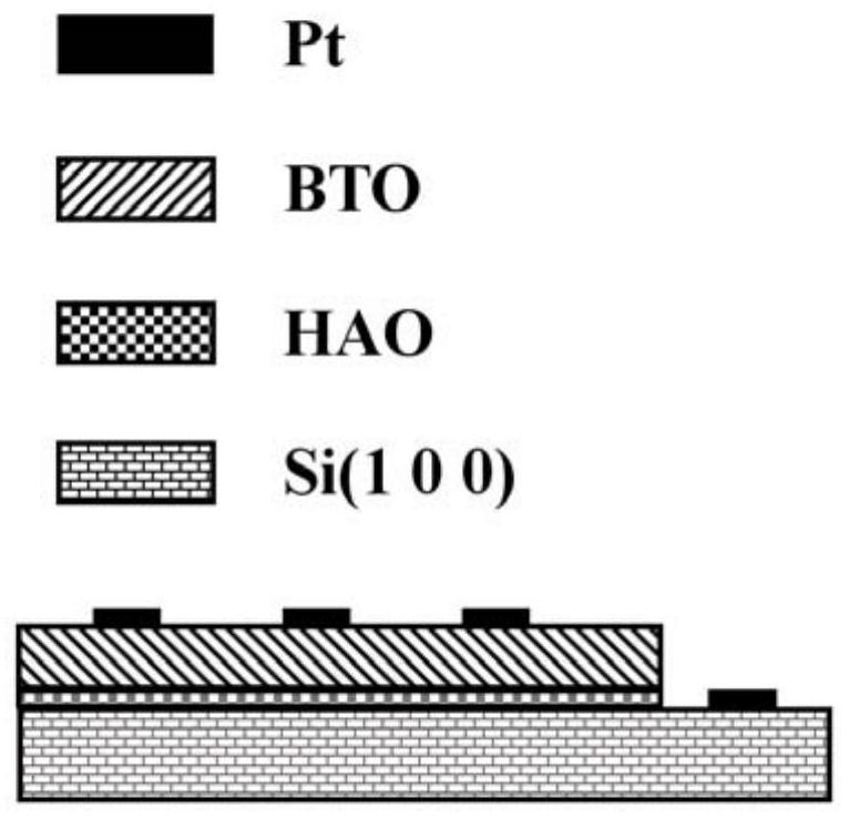
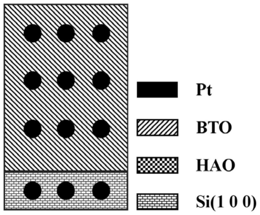
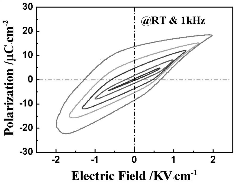
Examples
preparation example Construction
[0040]The preparation method of the silicon integrated BTO film of the present invention includes the following steps.
[0041](1) Si substrate processing
[0042]The Si substrate was immersed in hydrofluoric acid and deionized water successively for cleaning to remove impurities and natural oxide layer on the surface of the Si substrate, and then dried with high-pressure nitrogen and sent to the vacuum deposition chamber of the atomic layer deposition equipment. On the sample stage.
[0043](2) 8Al2O3:96HfO2Preparation of the transition layer
[0044]Using atomic layer deposition method to grow 8Al with preset thickness on Si substrate2O3:96HfO2Transition layer.
[0045](3)BaTiO3Film preparation
[0046]Using radio frequency magnetron sputtering method in 8Al2O3:96HfO2Fixed time growth of BaTiO on the transition layer3film. Radio frequency magnetron sputtering uses BaTiO3Target material, the background vacuum in the magnetron sputtering chamber is better than 10-5mbar, the working gas is a mixed gas...
Embodiment
[0050]The method for preparing the silicon integrated BTO film of this embodiment includes the following steps:
[0051](1) Si substrate processing
[0052]A P-type (100) Si wafer doped with boron is selected. Immerse briefly in hydrofluoric acid with a solute volume fraction of 2% to remove SiO on the surface of the Si substrate2Oxide layer and other impurities; then quickly rinse with deionized water to remove residual hydrofluoric acid; then use high-pressure nitrogen to dry the substrate and send it to the vacuum deposition chamber of the atomic layer deposition equipment and place it on the sample table.
[0053](2) 8Al2O3:96HfO2Transition layer preparation
[0054]Using atomic layer deposition method to grow 8Al with preset thickness on Si substrate2O3:96HfO2Transition layer. Using the conditions shown in Table 1, change HfO2Cycle and Al2O3Cyclic deposition sequence to grow HfO on Si substrate2:Al2O38Al with a cycle ratio of 96:8 and a thickness of 13nm2O3:96HfO2Transition layer.
[0055]Tab...
PUM
| Property | Measurement | Unit |
|---|---|---|
| thickness | aaaaa | aaaaa |
| thickness | aaaaa | aaaaa |
| thickness | aaaaa | aaaaa |
Abstract
Description
Claims
Application Information