Bridging system and bridging method for accessing Flash memory by RISCV processor

A memory and processor technology, applied in the direction of electrical digital data processing, instruments, etc., can solve the problems of large area consumption of bridge modules, RISCV processor and Flash memory cannot be interconnected, etc., to ensure work efficiency, realize high-speed reading, reduce The effect of development difficulty

Active Publication Date: 2021-01-08
NANJING UNIV
View PDF6 Cites 1 Cited by
  • Summary
  • Abstract
  • Description
  • Claims
  • Application Information

AI Technical Summary

Problems solved by technology

[0003] In the prior art, the RISCV processor and the Flash memory cannot be interconnected, and the traditional bridge module needs to rely on asynchronous FIFO to complete cross-clock domain signal processing, which consumes a large area of ​​the bridge module

Method used


Image

  • Bridging system and bridging method for accessing Flash memory by RISCV processor
  • Bridging system and bridging method for accessing Flash memory by RISCV processor
  • Bridging system and bridging method for accessing Flash memory by RISCV processor

Examples


Embodiment 1

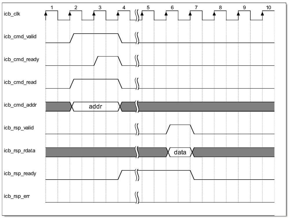
[0032] The read timing diagram of the ICB bus is as follows: figure 1 shown.

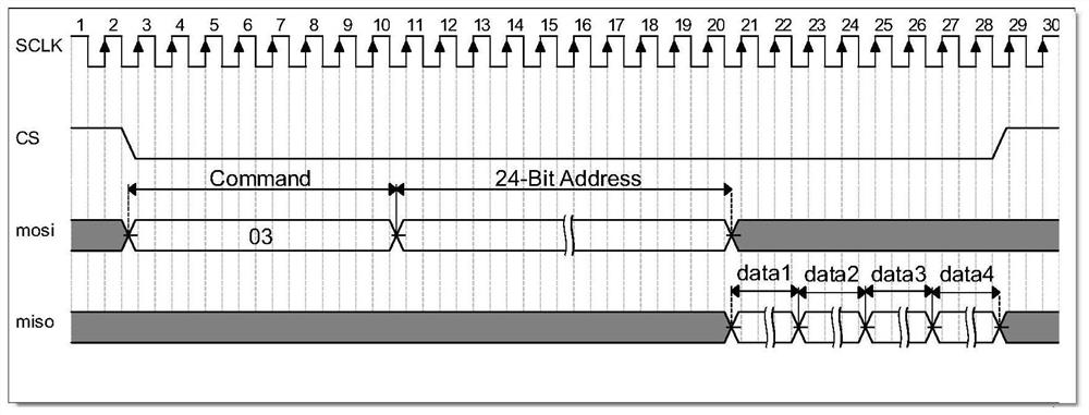
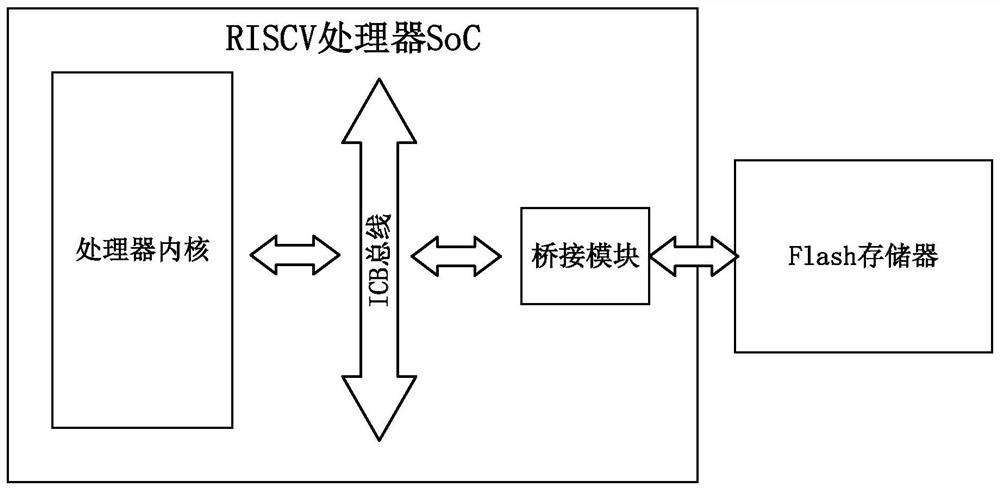
[0033] Flash memory usually adopts SPI bus interface. SPI is a serial peripheral interface, which has the characteristics of synchronous transmission, high transmission rate, full-duplex support, and simple communication method. The SPI bus is only composed of 1 clock line, 1 chip select line and 2 data lines, which can greatly reduce the pin requirements of the processor and reduce the area of ​​the processor. Both the master and slave devices of the SPI bus transmit data on the falling edge, and complete data sampling on the rising edge. The read timing of the Flash memory is as shown figure 2 shown. Described RISCV processor accesses the bridging module of Flash memory, is connected with the ICB bus of RISCV processor by ICB bus interface, is connected with external Flash memory by SPI bus interface, and bridge module realizes RISCV processing as a module of RISCV processor SoC Chip-to-chip i...

Embodiment 2

[0038] The ICB control module mainly works under the drive of the ICB state machine. The ICB state machine includes three states: ICB_IDLE, ICB_REQ, and ICB_WAIT: the ICB_IDLE state is the initial state. When the RISCV processor initiates a read request, the state machine changes from ICB_IDLE to ICB_REQ, and the module Register the control signal and read address signal, and generate a 1-beat ICB start signal; when the ICB end signal is sampled to be valid, the state machine changes from ICB_REQ to ICB_WAIT state, and the module returns the read data on the ICB bus; After the RISCV processor samples the read data, the state machine changes from the ICB_WAIT state to the ICB_IDLE state, waiting for the RISCV processor to initiate the next read request. The state transition of the ICB state machine is as follows Figure 5 shown.

[0039] The SPI control module mainly works under the drive of the SPI state machine. The SPI state machine includes three states: SPI_IDLE, SPI_SEND...

Embodiment 3

[0043] Based on the first and second embodiments above, the specific working process of the present invention is as follows: the interconnection between the RISCV processor and the bridge module is realized through the bus interface of the RISCV processor. The interconnection between the Flash memory and the bridge module is realized through the Flash memory bus interface. According to the requirements of the ICB bus protocol, it receives and responds to the read request initiated by the RISCV processor, and returns the data of the corresponding address of the Flash memory to the ICB control module.

[0044] After the read request initiated by the RISCV processor, the ICB control module starts, analyzes and registers the address and control signal of the ICB bus, and the generated ICB start signal is processed asynchronously by the ICB-SPI interactive module to obtain the SPI start signal, and the SPI start signal The SPI control module can be started. The SPI control module s...


PUM


Abstract

The invention provides a bridging system and a bridging method for accessing a Flash memory by an RISCV processor, which can realize high-speed reading of data of the Flash memory by the RISCV processor. The bridging system comprises an RISCV (Reduced Inter Standard Command Vector) processor bus interface, wherein the RISCV processor adopts a self-defined ICB (Integrated Circuit Bus) protocol; a Flash memory bus interface, wherein the Flash memory adopts an SPI (Serial Peripheral Interface) bus protocol; an ICB control module used for processing the bus transaction initiated by the RISCV processor; an SPI bus module used for initiating a bus transaction request to the Flash memory; and an IC-BSPI interaction module used for realizing signal interaction between the ICB control module and anSPI control module. Due to design of an asynchronous circuit, the RISCV processor and a Flash memory can work under the respective highest frequencies, so that working efficiency of the whole systemis ensured. Compared with a traditional bridging module, clock domain crossing signal processing is completed without asynchronous FIFO, and the area consumption of the bridging module can be reduced.

Description

technical field [0001] The invention relates to a bridging system and a bridging method for a RISCV processor to access a Flash memory, and relates to the field of system-on-chip (SoC) data transmission. Background technique [0002] After the processor is powered on, it needs to read a fixed initialization program, called the BIOS (Basic Input Output System) program. The BIOS program can help the processor complete the power-on self-test and the most basic configuration. The BIOS program is usually solidified in the read-only memory (ROM), but the processor usually uses a high-speed parallel bus, and the memory usually uses a low-speed serial bus. Different bus protocols are not compatible, and the processor cannot be directly connected to the memory to complete memory data processing. to read. Therefore, it is necessary to add a bridge module inside the processor to realize the conversion between the processor bus protocol and the memory bus protocol. [0003] In the pri...

Claims


Application Information

Patent Timeline
Patent Type & Authority Applications(China)
IPC IPC(8): G06F13/40G06F13/16G06F13/42
CPCG06F13/4068G06F13/1684G06F13/4295G06F13/4291
Inventor 李丽赵毅峰傅玉祥徐瑾沈思睿杨和平何书专陈铠
Owner NANJING UNIV
Why Eureka
Try Eureka