
P-n heterojunction based on organic two-dimensional molecular crystal, and preparation method and application thereof

A molecular crystal and heterojunction technology, applied in circuits, semiconductor/solid-state device manufacturing, electrical components, etc., can solve the problem of unreported application of organic two-dimensional molecular crystal single-phase half-wave rectifiers, and achieve the effect of simple and economical preparation method.

Pending Publication Date: 2021-01-08
TIANJIN UNIV
View PDF5 Cites 0 Cited by
  • Summary
  • Abstract
  • Description
  • Claims
  • Application Information

AI Technical Summary

Problems solved by technology

However, there is no report on the p-n heterojunction of organic two-dimensional molecular crystals and its gate-controllable rectification behavior and its application in single-phase half-wave rectifiers.

Method used


Image

  • P-n heterojunction based on organic two-dimensional molecular crystal, and preparation method and application thereof
  • P-n heterojunction based on organic two-dimensional molecular crystal, and preparation method and application thereof
  • P-n heterojunction based on organic two-dimensional molecular crystal, and preparation method and application thereof

Examples


Embodiment 1

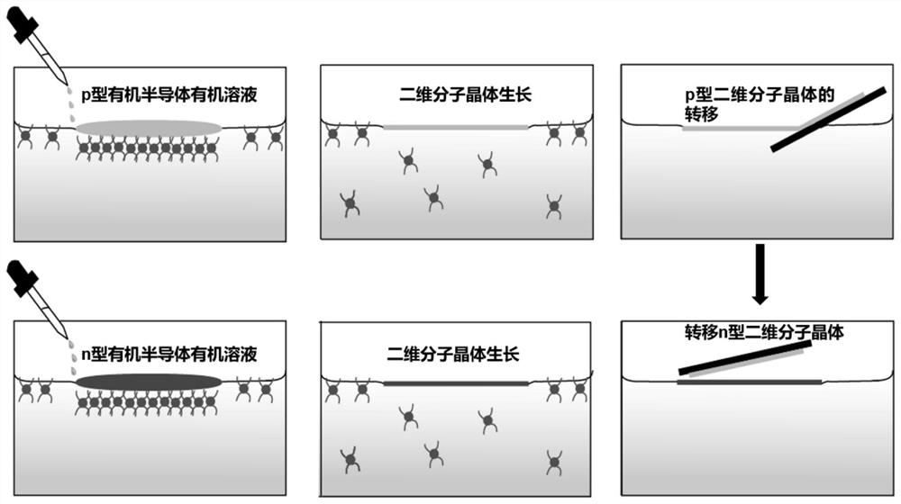
[0058] A p-n heterojunction based on organic two-dimensional molecular crystals, such as figure 1 shown, including the following steps:

[0059] Step 1: Add 100mg of tetrabutylammonium bromide and 10mL of ultrapure water into a weighing bottle with a diameter of 7cm, and ultrasonically dissolve tetrabutylammonium bromide for 15 minutes to obtain tetrabutylammonium bromide with a concentration of 10mg / mL Aqueous solution of ammonium bromide; add 1.5mg of 2,6-bis(4-hexylphenyl)anthracene (C6-DPA) into 1mL of toluene, sonicate for 20min to completely dissolve 2,6-bis(4-hexylphenyl)anthracene , to obtain an organic solution of 2,6-bis(4-hexylphenyl)anthracene with a concentration of 1.5mg / mL; Cover the surface of the ammonium chloride aqueous solution, cover the cap of the weighing bottle, and place it at room temperature at 20°C to 25°C to let the toluene slowly volatilize. ,6-bis(4-hexylphenyl)anthracene organic two-dimensional molecular crystal;

[0060] Step 2: Similarly, a...

Embodiment 2

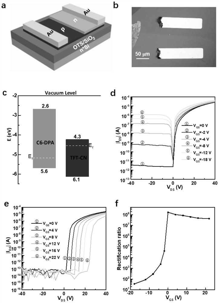
[0063] The p-n heterojunction based on the organic two-dimensional molecular crystal prepared in Example 1 is used to prepare a diode device, and the device structure is as follows figure 2 As shown in (a), the gold electrode is used as the source and drain electrodes, covering the p-type 2,6-bis(4-hexylphenyl)anthracene organic two-dimensional molecular crystal and the overlapping region of the heterojunction respectively; Si is used as the gate, 300nm thick SiO on the substrate 2 as a dielectric layer.

[0064] Among them, the preparation method of the gold electrode is as follows: first, the surface is covered with a thickness of 300nm SiO 2 A silicon wafer is used as a substrate, and the substrate is modified with octadecyltrichlorosilane, and then a copper mesh is used as a mask to paste on the substrate modified by octadecyltrichlorosilane, and the copper mesh is 100 × 400 inches The rectangular mask, the mesh number of the copper mesh is 200 mesh, and then A gold f...

Embodiment 3

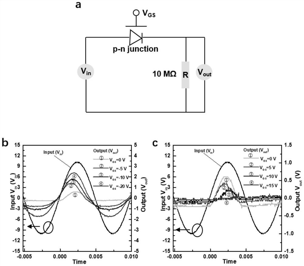
[0068] The organic two-dimensional molecular crystal-based p-n heterojunction diode device prepared in Example 2 was applied to a half-wave rectifier circuit.

[0069] The schematic diagram of the rectifier circuit is shown in image 3 As shown in (a), the method is as follows: one end of the p-n heterojunction diode device based on organic two-dimensional molecular crystals is electrically connected to a 10 megohm resistor, and the other end is electrically connected to a function signal generator and input sinusoidal waveform voltage (Vin) , an oscilloscope is connected in parallel at both ends of the resistance to read the output voltage signal (Vout) at the 10MΩ resistance; in addition, a source meter is used to apply a gate at the end of the p-n heterojunction diode device based on organic two-dimensional molecular crystals pressure.

[0070] The rectification circuit of the p-n heterojunction diode device based on the organic two-dimensional molecular crystal utilizes t...


PUM

PropertyMeasurementUnit
Resistivityaaaaaaaaaa

Abstract

The invention discloses a p-n heterojunction based on an organic two-dimensional molecular crystal, a vertically stacked p-n heterojunction with a p-type organic semiconductor two-dimensional molecular crystal at the lower part and an n-type organic semiconductor two-dimensional molecular crystal at the upper part is prepared by adopting a mechanical transfer method, and a gate-controllable rectification behavior is realized; and the application of the organic two-dimensional molecular crystal p-n heterojunction in a half-wave rectification circuit is realized by utilizing a simple rectification circuit. According to the invention, the two-dimensional organic molecular crystal can be transferred to any substrate by a method of mechanically transferring the two-dimensional molecular crystal, and the selection between materials is not limited by the transfer method, so that organic heterojunctions with different structures can be constructed.

Description

technical field [0001] The invention belongs to the technical field of two-dimensional organic single crystal heterojunction, and specifically relates to the preparation of two-dimensional organic single crystal heterojunction and its application in rectifier circuits. Background technique [0002] p-n semiconductor heterojunction structures are fundamental building blocks used in many important devices, including diodes, bipolar transistors, photodiodes, light-emitting diodes, and solar cells, among others. Among them, the p-n junction diode is the most common and basic component in modern electronics, and has a wide range of applications in the fields of integrated circuits, detectors, optoelectronics and lasers. Diodes based on p-n junctions have unidirectional conductivity, and this rectification characteristic has important application value in rectification circuits and switching circuits. In the traditional p-n homojunction, the p-type and n-type regions are chemical...

Claims


Application Information

Patent Timeline
IPC IPC(8): H01L51/05H01L51/40
CPCH10K10/26
Inventor 李荣金田馨孜牛智凯胡文平
Owner TIANJIN UNIV
Learn More