Organic light-emitting device containing carbazole as core compound and application of organic light-emitting device
An electroluminescent device and luminescent technology, applied in the direction of electric solid-state devices, electrical components, luminescent materials, etc., can solve the problems of low light extraction efficiency, reduce the angle dependence of the device, etc., and achieve high light extraction efficiency and excellent viewing angle , the effect of angle-dependent inhibition
- Summary
- Abstract
- Description
- Claims
- Application Information
AI Technical Summary
Problems solved by technology
Method used
Image

Examples
Embodiment 1
[0067] Embodiment 1: the synthesis of compound 8:
[0068]
[0069] Under nitrogen atmosphere, add 0.01mol raw material I-1, 0.025mol raw material II-1, 0.03mol sodium tert-butoxide, 5×10 -5 mol Pd 2 (dba) 3 and 5×10 -5 mol of tri-tert-butylphosphine, then add 150ml of toluene to dissolve it, heat to 100°C, reflux for 24 hours, observe the reaction by TLC until the reaction is complete. Naturally cooled to room temperature, filtered, and the filtrate was rotary evaporated until there was no fraction. The resulting material was purified by silica gel column (petroleum ether as eluent) to obtain Intermediate A-1.
[0070] In a 250ml three-neck flask, under the protection of nitrogen, add 0.01mol intermediate A-1, 0.015mol raw material III-1, 150ml toluene and stir to mix, then add 5×10 -5 mol Pd 2 (dba) 3 , 5×10⁻⁵mol P(t-Bu) 3 , heated to 110° C., and refluxed for 24 hours. The reaction was observed by TLC until the reaction was complete. Naturally cooled to room tem...
Embodiment 2
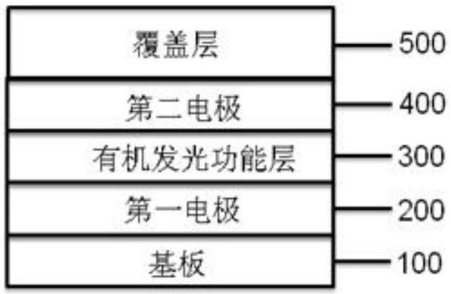
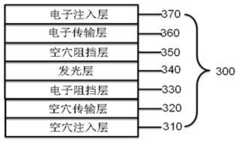
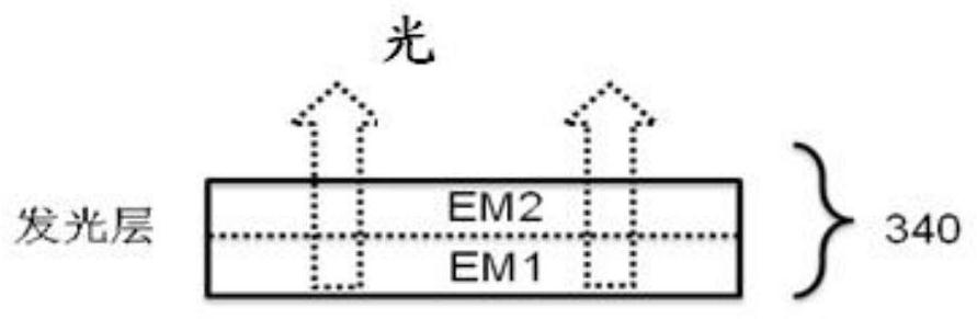
[0127] Transparent substrate layer 1 / anode layer 2 (ITO(15nm) / Ag(150nm) / ITO(15nm)) / hole injection layer 3(HT-1:P-1=97:3 mass ratio, thickness 10nm) / hole Hole transport layer 4 (HT-1, thickness 130nm) / electron blocking layer 5 (EB-2, thickness 40nm) / light-emitting layer 6 (GH-1:GH-2:GD-1=47:47:6 mass ratio, Thickness 40nm) / hole blocking / electron transport layer 7 (ET-1:Liq=1:1 mass ratio, thickness 35nm) / electron injection layer 8 (Yb, thickness 1nm) / cathode layer 9 (Mg:Ag=1: 9 mass ratio, thickness 15 nm) / CPL layer 10 (compound 8 of the present invention, thickness 70 nm).
Embodiment 3
[0129] Transparent substrate layer 1 / anode layer 2 (ITO(15nm) / Ag(150nm) / ITO(15nm)) / hole injection layer 3(HT-1:P-1=97:3 mass ratio, thickness 10nm) / hole Hole transport layer 4 (HT-1, thickness 130nm) / electron blocking layer 5 (EB-3, thickness 90nm) / light-emitting layer 6 (RH-1:RD-1=97:3 mass ratio, thickness 40nm) / hole Blocking / electron transport layer 7 (ET-1: Liq=1:1 mass ratio, thickness 35nm) / electron injection layer 8 (Yb, thickness 1nm) / cathode layer 9 (Mg:Ag=1:9 mass ratio, thickness 15nm ) / CPL layer 10 (compound 8 of the present invention, thickness 70 nm).
PUM
| Property | Measurement | Unit |
|---|---|---|
| Thickness | aaaaa | aaaaa |
Abstract
Description
Claims
Application Information