A new mems high q value non-solenoid integrated inductor and its preparation method

A technology integrating inductors and solenoids, applied in the field of microelectronics, can solve problems such as difficulty, high process cost, and subsequent packaging difficulties, and achieve the effects of suppressing substrate loss, reducing ohmic loss, and suppressing eddy current effects

Active Publication Date: 2022-03-18
FUDAN UNIV
View PDF0 Cites 0 Cited by
  • Summary
  • Abstract
  • Description
  • Claims
  • Application Information

AI Technical Summary

Problems solved by technology

[0007] However, the above-mentioned methods have various problems such as process complexity, inconvenient IC compatible integration, difficulty in subsequent packaging, insufficient mechanical stability, high process cost and difficulty, etc.

Method used


Image

  • A new mems high q value non-solenoid integrated inductor and its preparation method
  • A new mems high q value non-solenoid integrated inductor and its preparation method
  • A new mems high q value non-solenoid integrated inductor and its preparation method

Examples


Embodiment

[0062] Specific novel process for preparing high-Q MEMS non-inductance of the solenoid integrates the following:

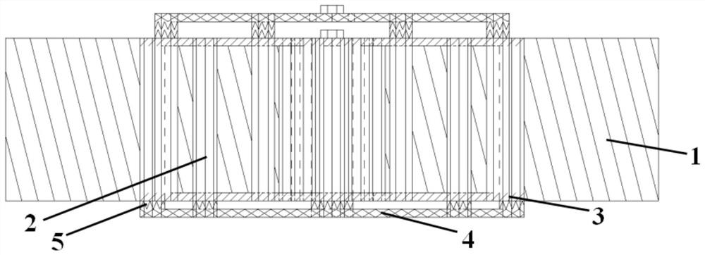
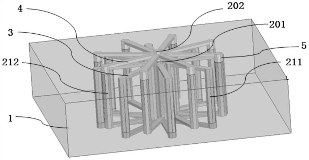
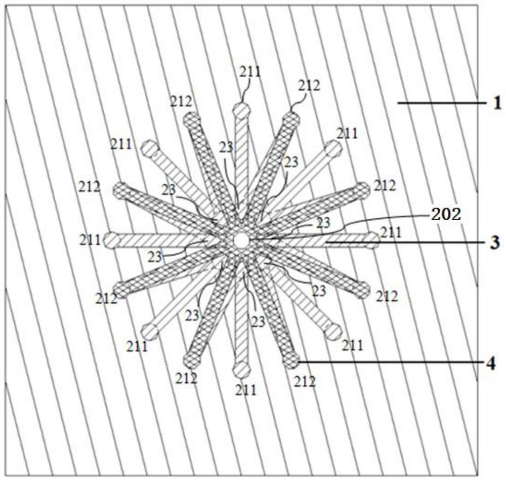
[0063] S1, such as Figure 3A , In 4-inch silicon wafer (silicon substrate 1) on the photoresist 6 is coated, prebaking, exposure, development, hard film-based SF6 / O 2 The method of low-temperature plasma etching reaction gas deep reactive ion etching (the DRIE) process on the silicon wafer etching to form a smooth steep sidewall 100μm deep TSV vias radius of 7.5μm shaped regular octagonal column, based on the sidewalls SiH 4 / O 2 Gas low pressure chemical vapor deposition (Low Pressure Chemical Vapor Deposition, referred to as LPCVD) depositing a layer of 1μm thick low temperature oxide layer (the LTO), for isolating the inductor and the silicon substrate, reduce the substrate loss. TSV thus forming micro-via holes of the inner: outer TSV microvia Number = 8: 2 * TSV via pattern 8. Wherein, inside the corresponding micro-vias TSV copper pillar inner group 23 micro,...


PUM

PropertyMeasurementUnit
thicknessaaaaaaaaaa

Abstract

The invention discloses a novel MEMS high-Q value non-solenoid integrated inductor and a preparation method thereof. The integrated inductor includes: a silicon substrate; a TSV micro-copper column embedded in the silicon substrate, and its two ends are respectively exposed. The TSV micro-copper column includes: a central port copper column, an inner micro-copper column group, a first outer micro-copper column group and a second outer micro-copper column group; a first surface layer interconnection coil, which includes a top surface layer interconnection coil, a bottom layer a skin interconnection coil; a skin interconnection copper pillar; and, a second skin interconnection coil comprising a top skin interconnection coil and a bottom skin interconnection coil. The invention adopts an improved embedded non-solenoid integration scheme, isolates the inductor and the silicon substrate through a low-temperature oxide layer, reduces the loss of the substrate, and supports the non-solenoid structure surface layer interconnection coil through an insulating material, in a small area Embedded with integrated multi-turn coils, it finally forms a micro-integrated inductor with low loss, small stray parasitic capacitance, and high Q value. It is also compatible with the packaging process and mechanically stable.

Description

Technical field [0001] The present invention relates to the integrated passive element in the field of microelectronics, and more particularly to a novel MEMS high Q value non-solenoid integrated inductance of peak quality factor Q to 40. Background technique [0002] In the past 30 years, with the development of electronic communication technology, the function of intelligent consumer electronics is increasing, inductance as basic and necessary electronic components, is widely used in integrated circuits, such as matching networks, filters, low noise amplifiers. , Transceiver, voltage controlled oscillator, etc. Conventional discrete inductors have no longer satisfying the urgent needs of small-size and low power consumption, with low energy consumption, small size, low noise, and high-frequency segment induction, low-end noise, and high-frequency demand. Increase. Quality factor Q is one of the important indicators of the quality of the inductance, the smaller the Q value, the ...

Claims


Application Information

Patent Timeline
Patent Type & Authority Patents(China)
IPC IPC(8): H01F27/28H01F27/30H01F41/00H01F41/18H01F41/22
CPCH01F41/00H01F41/18H01F41/22H01F27/2866H01F27/2871H01F27/303
Inventor 周盛锐徐玲杨颖琳
Owner FUDAN UNIV
Why Eureka
Try Eureka