Method for manufacturing GaP rough surface of GaAs-based LED wafer

A production method and rough surface technology, which is applied in the field of semiconductor processing optoelectronics, can solve the problems of difficult control of corrosion rate and uniformity of corrosion, large limitation of brightness improvement, large difference of brightness between regions, etc., to achieve easy control and light extraction efficiency Enhanced, high usability effects

Active Publication Date: 2021-02-23
SHANDONG INSPUR HUAGUANG OPTOELECTRONICS
View PDF4 Cites 2 Cited by
  • Summary
  • Abstract
  • Description
  • Claims
  • Application Information

AI Technical Summary

Problems solved by technology

However, this invention still adopts the conventional roughening wet etching method. As long as the solution is used for etching, the roughening corrosion rate will be faster due to its own nature. Generally, the etching can be completed in tens of seconds to a few minutes. The rate and uniformity of corrosion are difficult to control, the roughened surface pore structure formed is relatively shallow, and the improvement of brightness by solution roughening is relatively limited
[0005] Chinese patent CN105895750A (201610274404.9) proposes a method for preparing a GaP rough surface of a quaternary chip. The method is as follows: the GaP surface is subjected to sandblasting roughening treatment and wet etching treatment in order to obtain a GaP rough light emitting surface In this invention, holes and defective GaP surfaces are obtained by sandblasting, and the surface is roughened by conventional chemical etching methods. In this invention, deep and stable pore structures can be obtained by sandblasting and chemical etching, and the brightness improvement is more obvious. , but the sandblasting treatment has uncertainty, the hole shape of the overall roughened area is uneven, and the brightness varies greatly by area

Method used


Image

  • Method for manufacturing GaP rough surface of GaAs-based LED wafer
  • Method for manufacturing GaP rough surface of GaAs-based LED wafer
  • Method for manufacturing GaP rough surface of GaAs-based LED wafer

Examples


Embodiment 1

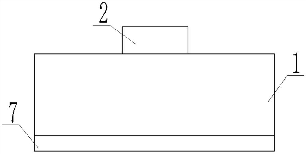
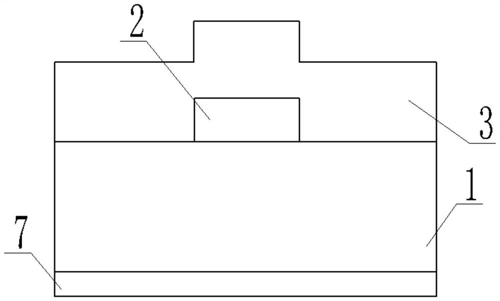
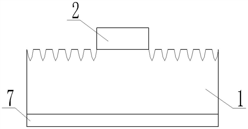
[0062] S1: Epitaxial layer 1 growth: Prepare the epitaxial layer 1 growth material, and check the operation of each device; then take the GaAs substrate 7, and grow a buffer layer and an N-type gallium arsenide layer on the GaAs substrate 7 from bottom to top in sequence , DBR layer, N-type confinement layer, MQW quantum well layer, P-type confinement layer, P-type GaP, GaP window layer, to obtain the epitaxial layer 1 of the wafer;

[0063] S2: Preparation of P-electrode protective layer 2: take the prepared wafer with epitaxial layer 1, grow a silicon dioxide layer on the GaP window layer, perform photolithography, and wet-etch away the silicon dioxide layer outside the P-face electrode 5 area , to obtain the P electrode protective layer 2; wherein the thickness of the silicon dioxide layer is The growth temperature is 200°C;

[0064] S3: Prepare corrosion sol; take photoresist, roughening etchant and surfactant, and mix them uniformly in proportion to prepare corrosion so...

Embodiment 2

[0071] S1: Epitaxial layer 1 growth: Prepare the epitaxial layer 1 growth material, and check the operation of each device; then take the GaAs substrate 7, and grow a buffer layer and an N-type gallium arsenide layer on the GaAs substrate 7 from bottom to top in sequence , DBR layer, N-type confinement layer, MQW quantum well layer, P-type confinement layer, P-type GaP, GaP window layer, to obtain the epitaxial layer 1 of the wafer;

[0072] S2: Preparation of P-electrode protective layer 2: take the prepared wafer with epitaxial layer 1, grow a silicon dioxide layer on the GaP window layer, perform photolithography, and wet-etch away the silicon dioxide layer outside the P-face electrode 5 area , to obtain the P electrode protective layer 2; wherein the thickness of the silicon dioxide layer is The growth temperature is 225°C;

[0073] S3: Preparation of corrosion sol; take photoresist, roughening corrosion solution and surfactant, and mix them uniformly in proportion to pr...

Embodiment 3

[0080] S1: Epitaxial layer 1 growth: Prepare the epitaxial layer 1 growth material, and check the operation of each device; then take the GaAs substrate 7, and grow a buffer layer and an N-type gallium arsenide layer on the GaAs substrate 7 from bottom to top in sequence , DBR layer, N-type confinement layer, MQW quantum well layer, P-type confinement layer, P-type GaP, GaP window layer, to obtain the epitaxial layer 1 of the wafer;

[0081] S2: Preparation of P-electrode protective layer 2: take the prepared wafer with epitaxial layer 1, grow a silicon dioxide layer on the GaP window layer, perform photolithography, and wet-etch away the silicon dioxide layer outside the P-face electrode 5 area , to obtain the P electrode protective layer 2; wherein the thickness of the silicon dioxide layer is The growth temperature is 250°C;

[0082] S3: Preparation of corrosion sol; take photoresist, roughening corrosion solution and surfactant, and mix them uniformly in proportion to pr...


PUM

PropertyMeasurementUnit
thicknessaaaaaaaaaa

Abstract

The invention discloses a method for manufacturing a GaP rough surface of a GaAs-based LED wafer, and the method comprises the steps: preparing a wafer epitaxial layer, carrying out the roughening corrosion of a GaP window layer of the epitaxial layer, dissolving photoresist and roughening corrosion liquid together through a surfactant, forming corrosion sol with a roughening corrosion effect, coating the surface of the GaP window layer with the corrosion sol, baking at a constant temperature of 40-60 DEG C, removing a corrosion film layer and a silicon dioxide layer by using solvents such asacetone and the like, and continuously preparing to obtain an independent tube core; the process method designed by the invention is simple and easy to operate, does not need to introduce special equipment, is lower in cost, is more uniform in coarsening corrosion of the surface of the epitaxial layer, is higher in corrosion controllability, is good in coarsening effect, and solves the problems that the coarsening corrosion is more difficult to control and the coarsening brightness is not improved greatly when a solution is used at present. When the method provided by the invention is used forcoarsening, the light extraction efficiency can be improved by 25-30 percent, and the method has higher practicability.

Description

technical field [0001] The invention relates to the technical field of semiconductor processing optoelectronics, in particular to a method for manufacturing a GaAs-based LED chip GaP rough surface. Background technique [0002] A light-emitting diode, referred to as LED (Light Emitting Diode), is a solid-state electroluminescent (EL) semiconductor device that converts electrical energy into light energy. Gallium arsenide is a typical direct transition energy band structure material. The minimum value of the conduction band and the maximum value of the valence band are both in the center of the Brillouin zone, which makes it have a high electro-optical conversion efficiency and is ideal for preparing optoelectronic devices. of excellent materials. Compared with traditional silicon semiconductor materials, gallium arsenide materials have many advantages such as high electron mobility, large band gap, direct band gap, and low power consumption. The electron mobility is about 5...

Claims


Application Information

Patent Timeline
Patent Type & Authority Applications(China)
IPC IPC(8): H01L33/22H01L33/00
CPCH01L33/0062H01L33/22
Inventor 徐晓强张兆喜王梦雪闫宝华徐现刚
Owner SHANDONG INSPUR HUAGUANG OPTOELECTRONICS
Why Eureka
Try Eureka