Cast single crystal seed crystal laying method with short bottom red area and few native dislocations
A laying method and single crystal technology, which are applied in the directions of single crystal growth, single crystal growth, chemical instruments and methods, etc., can solve the lattice distortion of silicon crystal, the side length of the red zone at the bottom of the cast single crystal silicon ingot, and the stress concentration. And other issues
- Summary
- Abstract
- Description
- Claims
- Application Information
AI Technical Summary
Problems solved by technology
Method used
Image
Examples
Embodiment 1
[0046] Example 1: Production of cast single crystal silicon ingots by conventional casting single crystal seed laying method (comparative example)
[0047] S11. Remove the head, tail and edge of the Czochralski monocrystalline silicon rod, and wire-cut it to obtain a cast single crystal seed crystal. The size of each cast single crystal seed crystal is 158mm×158mm×25mm. Wash the cast single crystal seed crystal with pure water first. Remove surface dirt, then clean with acid or lye to remove mechanical damage on the surface of the seed crystal, and finally wash away residual acid or lye with pure water;
[0048]S12. Pickling the scrapped silicon wafers, laying a layer of scrapped silicon wafers on the bottom of the crucible, the size of the silicon wafers is 158mm×158mm×0.18mm, and laying a layer of cast single crystal seed crystals on the silicon wafers;
[0049] S13. laying 25 pieces of cast single crystal seed crystals on the first thick layer, and closely bonding between a...
Embodiment 2
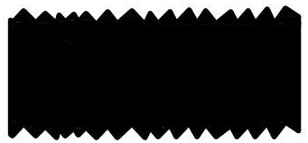
[0052] S21. Remove the head, tail and edge of the Czochralski monocrystalline silicon rod, and wire-cut it to obtain a cast single crystal seed crystal. The size of each cast single crystal seed crystal is 158mm×158mm×25mm. The upper and lower surfaces of the cast single crystal seed crystal are Sandblasting to increase its roughness, with a roughness value of 50 microns, such as figure 2 shown;
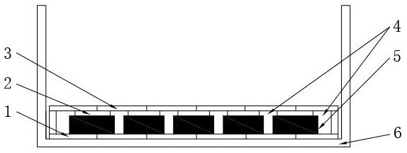
[0053] S22. Cut a slab from a polycrystalline silicon block or a monocrystalline silicon block, the slab size of the first slab layer and the third slab layer is 158mm×158mm×3mm, and the slab size of the second slab layer is 145mm× 145mm×3mm, sandblasting the upper and lower surfaces of the thick sheet to increase its roughness, the roughness value is 50 microns, such as image 3 shown;
[0054] S23. Laying 36 slabs on the bottom of the crucible, the sides of adjacent slabs are closely attached to form the first slab, the first slab covers the entire bottom of the crucible, and th...
PUM
 Abstract
Description
Claims
Application Information


