Solar cell capable of reducing cutting loss and preparation method
A technology for solar cells and batteries, applied in the field of solar cells, can solve the problems of increased compound current in the edge region, loss of efficiency of small cells, and reduced open voltage, etc., and achieves the effects of excellent effect, high efficiency concentration, and improved utilization rate.
- Summary
- Abstract
- Description
- Claims
- Application Information
AI Technical Summary
Problems solved by technology
Method used
Image
Examples
Embodiment 1
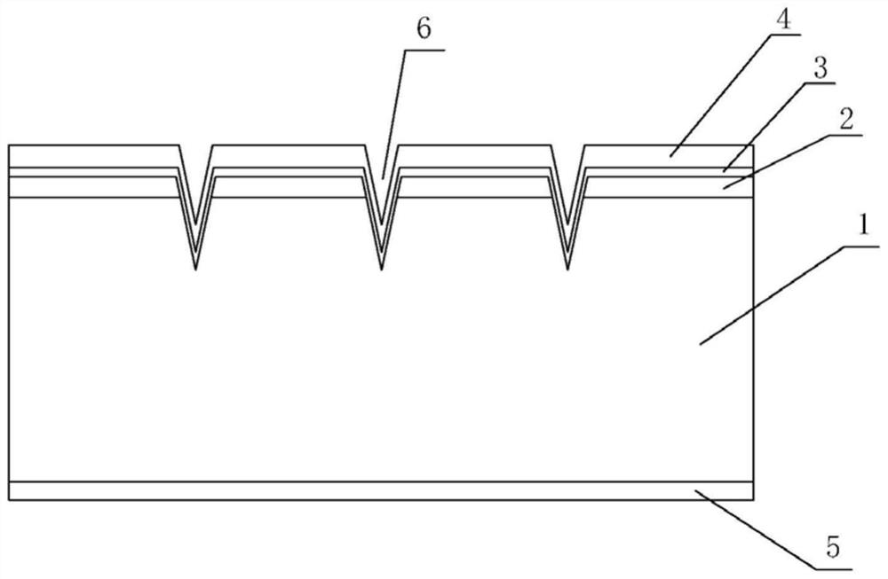
[0054] A solar cell that can reduce cutting loss. Four strip-shaped pre-cut windows are pre-set on the side of the silicon wafer with the emitter by laser scribing, and the obtained finished solar cells are divided into solar cells along the pre-cut windows Four stick battery cells. The preparation process comprises the following steps:
[0055] Take a textured p-type silicon wafer 1 with a thickness of 200um for diffusion and junction, and make an n-emitter 2 on the surface of the silicon wafer, and at the same time deposit a layer of phosphosilicate glass on the surface of the silicon wafer after diffusion;
[0056] A groove with a depth of 5um is formed on the surface of the silicon wafer 1 with the n-emitter 2 by laser scribing, and three V-shaped strip-shaped pre-cut windows 6 are arranged on the surface of the silicon wafer;
[0057] The silicon wafer 1 with the pre-cut window 6 on the surface is cleaned with NaOH solution, and the NaOH solution reacts with the PN junct...
Embodiment 2
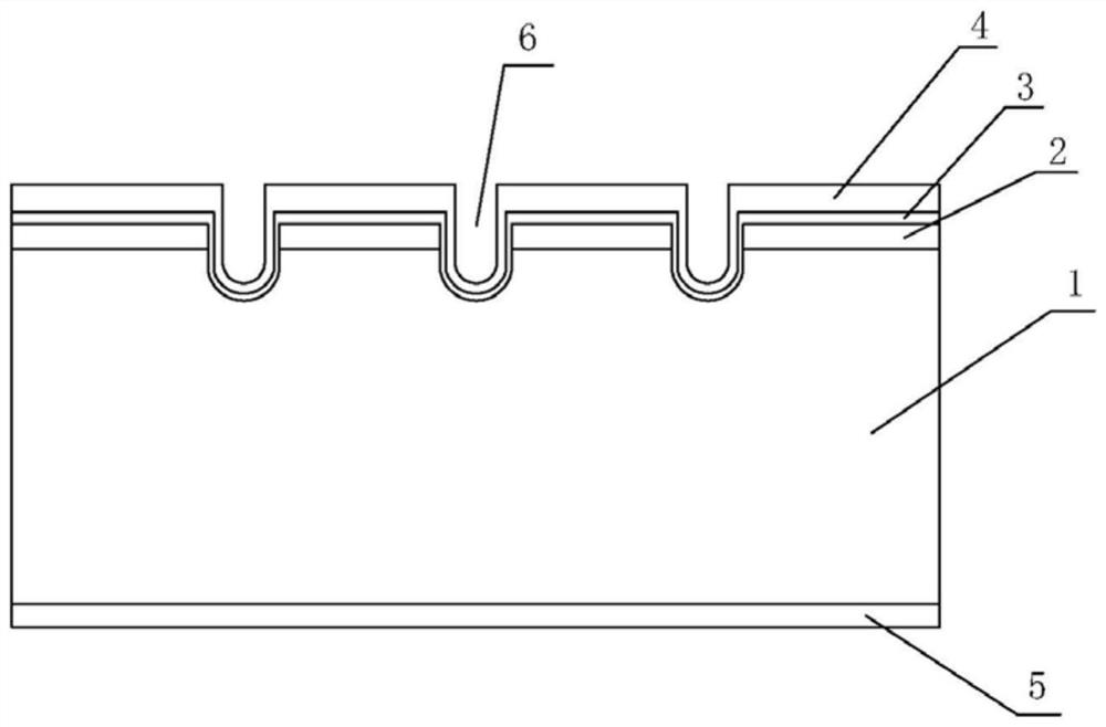
[0061] A solar cell capable of reducing cutting losses. Four strip-shaped pre-cut windows are pre-set on the side of the silicon wafer with the emitter electrode by screen printing corrosion paste, and the obtained finished solar cells are cut along the pre-cut windows. The battery is split into four strip cells. The preparation process comprises the following steps:
[0062] Take a textured p-type silicon wafer 1 with a thickness of 180um for diffusion and junction, and make an n-emitter 2 on the surface of the silicon wafer, and deposit a layer of phosphosilicate glass on the surface of the silicon wafer after diffusion;
[0063] On the surface of the silicon wafer 1 with the n-emitter 2, a groove with a depth of 2-5 um is formed by screen printing etching paste. In this embodiment, the depth of the groove is 3 um, and three U-shaped strips are arranged on the surface of the silicon wafer. Shaped pre-cut window 6; wherein the composition of the etching slurry includes ammon...
Embodiment 3
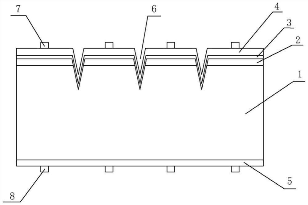
[0068] A solar cell that can reduce cutting loss. Four strip-shaped pre-cut windows are pre-set on the surface of the original silicon wafer by laser scribing. The obtained finished solar cell is divided into four strip-shaped cells along the pre-cut window. unit. The preparation process comprises the following steps:
[0069] Take the original P-type silicon wafer with a thickness of 200um, use laser scribing to form grooves with a depth of 10um on the front of the silicon wafer, and set three V-shaped strip-shaped pre-cut windows on the surface of the silicon wafer for texturing;
[0070] Diffusion of the silicon wafer to prepare the emitter on the surface of the silicon wafer;
[0071] Polish the silicon wafer on the back, oxidize the front to form an oxide layer, plate the front passivation anti-reflection film and the back passivation film, laser groove the back, print the positive electrode and the back electrode, and sinter to make PERC solar cells;
[0072] Take the ...
PUM
| Property | Measurement | Unit |
|---|---|---|
| thickness | aaaaa | aaaaa |
Abstract
Description
Claims
Application Information


