Check patentability & draft patents in minutes with Patsnap Eureka AI!

Preparation method of semiconductor material, perovskite semiconductor device and preparation method of perovskite semiconductor device

A semiconductor and perovskite technology, applied in the field of semiconductor optoelectronics, can solve the problems of low solar cell efficiency, large interface impedance, and many interface defects, and achieve the effects of increased charge collection efficiency, increased contact area, and good interface energy level matching.

Pending Publication Date: 2021-03-12
PEKING UNIV SHENZHEN GRADUATE SCHOOL
View PDF7 Cites 1 Cited by
  • Summary
  • Abstract
  • Description
  • Claims
  • Application Information

AI Technical Summary

Problems solved by technology

In the prior art, carbon electrode perovskite solar cells are prepared by directly coating carbon paste on the surface of the perovskite film. A good combination is formed between the perovskite and the carbon paste, and the long-term stability of the battery is good, but there are The disadvantage is that there are many interface defects and large interface impedance between the carbon electrode and the perovskite active layer, and the prepared solar cells have low efficiency and poor stability.

Method used


Image

  • Preparation method of semiconductor material, perovskite semiconductor device and preparation method of perovskite semiconductor device
  • Preparation method of semiconductor material, perovskite semiconductor device and preparation method of perovskite semiconductor device
  • Preparation method of semiconductor material, perovskite semiconductor device and preparation method of perovskite semiconductor device

Examples


Embodiment 1

[0039] This embodiment provides a MAPbI 3 The preparation method of perovskite semiconductor material is prepared according to the following steps:

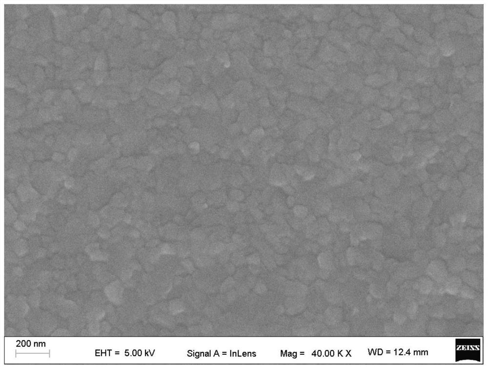
[0040] Take 60mg / mL lead acetate solution, the solvent is acetic acid, spin-coat at 2000rpm for 30 seconds on a common glass substrate, and then spin-coat 30mg / mL MAI (methylamine hydroiodide) solution, the solvent is isopropanol , spin-coating at 2000 rpm for 30 seconds, and heated at 100 °C for 10 minutes to obtain dense and smooth MAPbI 3 Perovskite thin films with surface microstructures such as figure 1 shown.

Embodiment 2

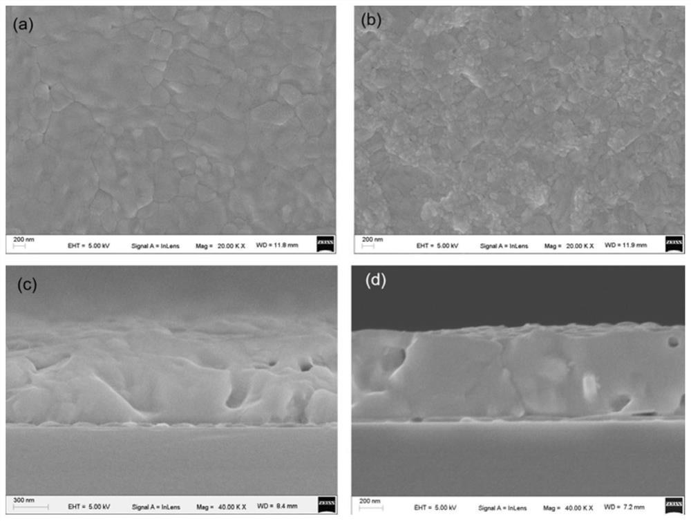
[0042] First, MAPbI prepared on ordinary glass substrates 3 Substrate: PbI 2and MAI were dissolved in DMSO and DMF, the volume ratio was 7:3, the concentration was 1.47M, the anti-solvent was a mixture of toluene and ethyl acetate, the volume ratio was 7:3, the rotation speed was 1000rpm 20s, and 2000rpm 50s, at the end Add the anti-solvent dropwise for 10 seconds, then heat at 60°C for 2 minutes, and continue heating at 100°C for 5 minutes to obtain a perovskite substrate.

[0043] Prepare another layer of perovskite film on the obtained perovskite substrate: get 15mg / mL of MAI (methylamine hydroiodide) solution, the solvent is isopropanol, spin-coat for 30 seconds with the rotating speed of 2000rpm, then take 18mg / mL lead acetate solution, the solvent is acetic acid, spin-coated on the perovskite substrate at a speed of 2000rpm for 30 seconds, and then spin-coated 15mg / mL MAI (methylamine hydroiodide) solution, the solvent is iso propanol, spin-coated at 2000 rpm for 30 s,...

Embodiment 3

[0045] This embodiment provides a FA 1-x MA x PB 3 The preparation method of the perovskite semiconductor material is prepared according to the following steps:

[0046] Get 18mg / mL of lead acetate solution, the solvent is a mixture of acetic acid and ethanol, the ratio is 5 to 5, spin coating with 1000rpm rotating speed for 60 seconds on the PET substrate, spin coating 30mg / mL FAI (a A mixed solution of amidine iodine) and MAI, the solvent is isopropanol, spin-coated at a speed of 1000rpm for 60 seconds, heated at 150°C for 10 minutes to obtain FA 1-x MA x PB 3 perovskite thin film.


PUM

PropertyMeasurementUnit
Short circuit current densityaaaaaaaaaa

Abstract

The invention discloses a preparation method of a semiconductor material, a perovskite semiconductor device and a preparation method of the perovskite semiconductor device. The preparation method of the semiconductor material comprises the following steps of depositing a carboxylate solution, wherein the carboxylate solution is selected from at least one of a lead carboxylate solution and a tin carboxylate solution; depositing an organic amine salt / amidine salt solution; annealing at 50 DEG C to 160 DEG C. According to the method, carboxylate and organic amine salt / amidine salt are used as rawmaterials, the used solvent does not contain DMF, DMSO and other strong-polarity toxic solvents, and the method is suitable for growing perovskite on various substrates sensitive to polar solvents and insensitive to polar solvents and is environmentally friendly. In addition, a carboxylate solution and an organic amine salt / amidine salt solution are used as perovskite precursor materials and arecrystallized in a carbon electrode, so that the carbon electrode material in direct contact with the perovskite layer is wrapped by the perovskite material, the contact area of perovskite / carbon heterojunctions is increased, and the photoelectric conversion performance and stability of the device are improved.

Description

technical field [0001] The invention relates to the technical field of semiconductor optoelectronics, in particular to a preparation method of a semiconductor material, a perovskite semiconductor device and a preparation method thereof. Background technique [0002] The preparation method of semiconductor material often determines its scope of use and application. The current solution methods for preparing perovskite thin films require the substrate to be insensitive to polar solvents, and use highly polar DMF, DMSO and other toxic solvents, which will adversely affect the environment in future industrial production. For example, in the anti-solvent method currently used to prepare high-quality perovskites, the solvents for dissolving perovskite precursor salts are mostly DMF and DMSO, which are strong polar solvents and are not suitable for growth on polar solvent-sensitive substrates. In addition, the perovskite precursor salt in the prior art also uses lead iodide, and l...

Claims


Application Information

Patent Timeline
IPC IPC(8): H01L51/46H01L51/48H01L51/42
CPCH10K71/12H10K71/40H10K85/30H10K30/00Y02E10/549
Inventor 杨世和刘通发
Owner PEKING UNIV SHENZHEN GRADUATE SCHOOL
Features
  • R&D
  • Intellectual Property
  • Life Sciences
  • Materials
  • Tech Scout
  • Unparalleled Data Quality
  • Higher Quality Content
  • 60% Fewer Hallucinations
Learn More