Preparation method of tunable FP optical filter based on film bonding
A filter and thin film technology, applied in the field of preparation of tunable FP filters, can solve the problems of difficult process and low yield, achieve high electro-optic coefficient, good temperature stability, and improve processing technology. high effect
- Summary
- Abstract
- Description
- Claims
- Application Information
AI Technical Summary
Problems solved by technology
Method used
Image
Examples
preparation example Construction
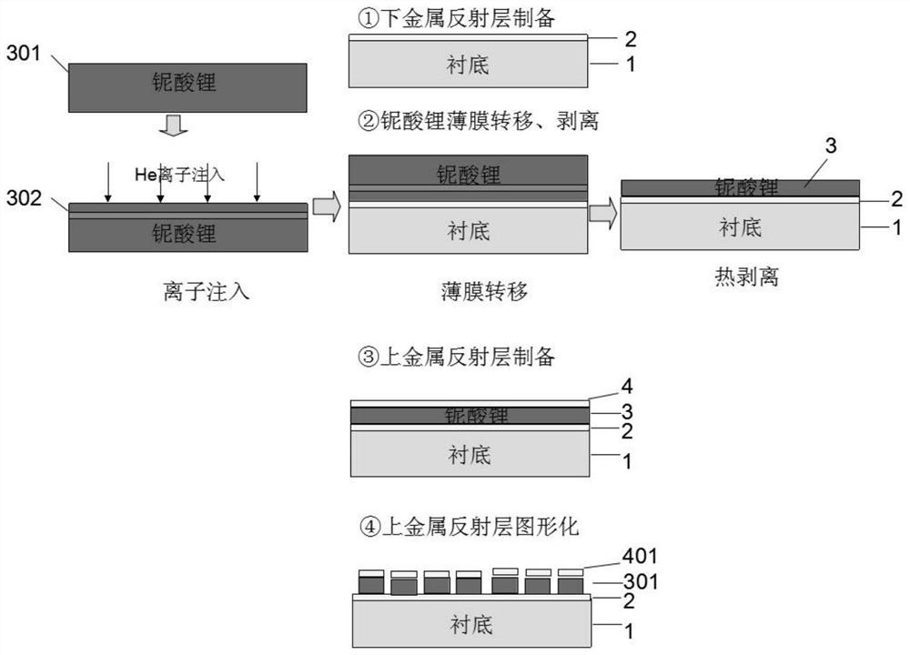
[0037] In order to solve the problems of the prior art, the present invention provides a method for preparing a tunable FP filter based on thin film bonding, such as figure 1 As shown, the method includes the following steps:
[0038] Step 1: Make the lower metal reflective layer;
[0039] The lower metal reflection layer of the FP filter is prepared by thermal evaporation coating method on the substrate;
[0040] Step 2: Preparation of the light-transmitting layer of the lithium niobate thin film:
[0041] The light-transmitting layer of lithium niobate thin film was prepared by ion implantation and bonding stripping method;
[0042] Step 3: Prepare the upper metal reflective layer:
[0043] The upper metal reflective layer is prepared by the method of magnetron sputtering;
[0044] Step 4: Patterning preparation of the upper metal reflective electrode:
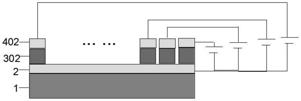
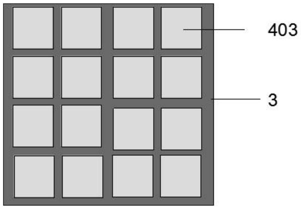
[0045] The upper metal electrode structure is fabricated by photolithography and ion beam etching process, and the tu...
Embodiment 1
[0058] like figure 1 As shown, this embodiment provides a method for preparing a tunable FP filter based on thin film transfer bonding, including the following steps:
[0059] ①The production of the lower metal reflection layer 2: Quartz glass, K9 glass or other highly transparent glass materials are firstly selected as the substrate 1; The material is Al, Ag, etc., and the reflectivity is required to be better than 90%;
[0060] ②Preparation of the light-transmitting layer 3 of the lithium niobate thin film: firstly, H ion implantation is performed on the surface of 301 on the lithium niobate substrate, and the lithium niobate implanted surface is bonded to the lower metal reflective layer 2 in the substrate 1 at the wafer level. The lithium niobate substrate 301 is removed by a thermal stripping method, leaving a bonded structure substrate with the lithium niobate film 3 and the lower metal reflective layer 2 to obtain the lithium niobate film light-transmitting layer 3;
...
PUM
| Property | Measurement | Unit |
|---|---|---|
| reflectance | aaaaa | aaaaa |
Abstract
Description
Claims
Application Information


