Fabrication method of gan-based hemt devices

A device and wafer technology, applied in the semiconductor field, can solve the problems of poor device performance and high device fabrication cost, and achieve the effects of improving performance, expanding application scope and reducing costs

Active Publication Date: 2022-05-17
SHANGHAI INST OF MICROSYSTEM & INFORMATION TECH CHINESE ACAD OF SCI
View PDF5 Cites 0 Cited by
  • Summary
  • Abstract
  • Description
  • Claims
  • Application Information

AI Technical Summary

Problems solved by technology

[0006] In view of the shortcomings of the prior art described above, the object of the present invention is to provide a method for preparing a GaN-based HEMT device, which is used to solve the problems of poor device performance and device preparation cost faced in the preparation of GaN-based HEMT devices in the prior art high problem

Method used


Image

  • Fabrication method of gan-based hemt devices
  • Fabrication method of gan-based hemt devices
  • Fabrication method of gan-based hemt devices

Examples


preparation example Construction

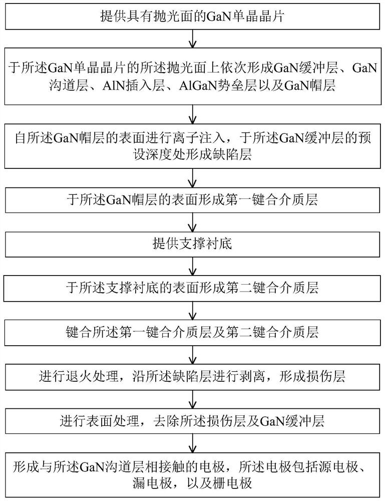
[0063] refer to figure 1 , the present invention provides a method for preparing a GaN-based HEMT device, which can transfer a high-quality AlGaN / GaN structure homoepitaxially on a self-supporting GaN single crystal substrate to a supporting substrate, and remove the residual layer on the surface after simple treatment. High-performance GaN-based HEMT devices can be obtained by growing source, drain, and gate electrodes; the self-supporting GaN single crystal substrate has no loss and can be recycled, thereby greatly reducing costs; according to the material characteristics of different supporting substrates, GaN can be realized The heterogeneous integration of the GaN-based HEMT device and the supporting substrate takes advantage of the different advantages of the GaN-based HEMT device to improve the performance of the GaN-based HEMT device, so that the GaN-based HEMT device can work stably for a long time under high frequency and high power conditions; further It can be appl...

Embodiment 1

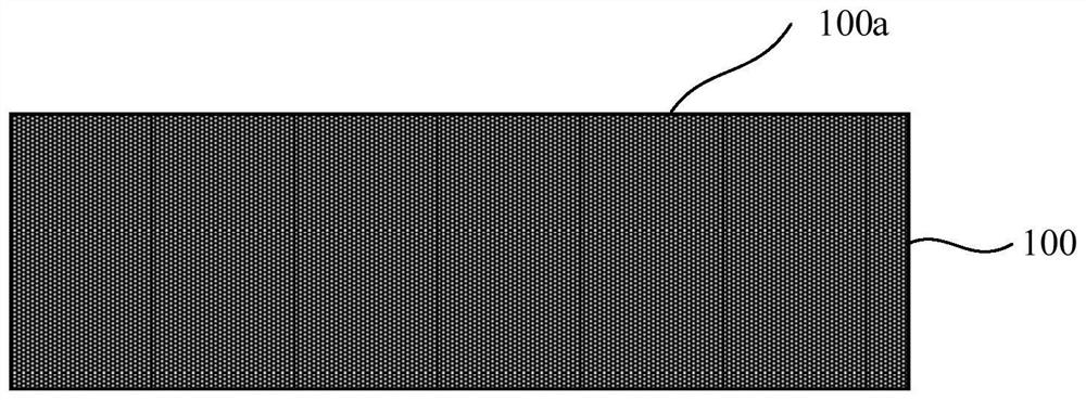
[0095] like figure 2 As shown, a GaN single crystal wafer 100 with a diameter of 2 inches, a thickness of 350 μm, and a (0001) crystal orientation Ga surface polishing is firstly provided.

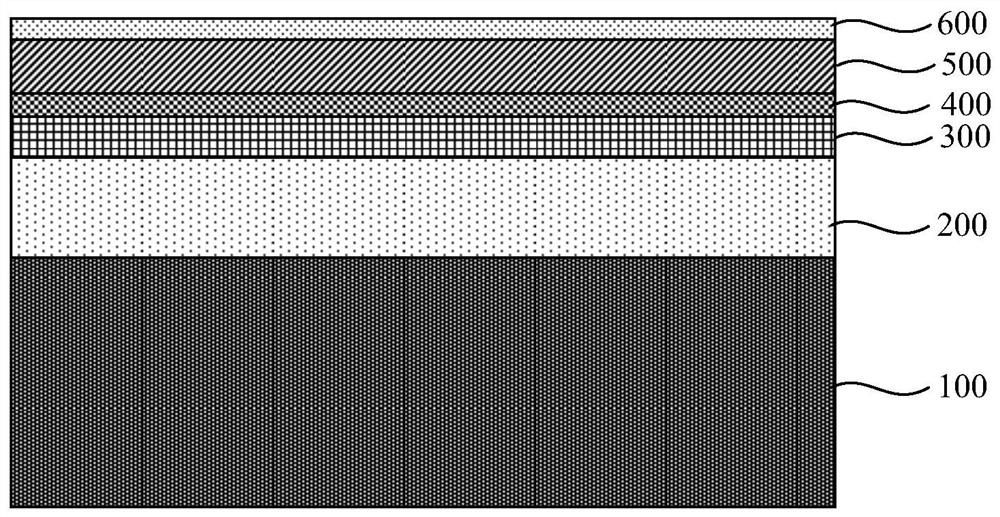
[0096] like image 3 As shown, on the polished surface 100a of the GaN single crystal wafer 100, a 2 μm thick GaN buffer layer 200, a 100 nm thick GaN channel layer 300, and a 1 nm thick AlN insertion Layer 400, 25nm thick Al X Ga 1-X N barrier layer 500, where x=0.25, 2nm thick GaN cap layer 600; constitute the first composite structure.

[0097] like Figure 4 , performing H ion implantation on the first composite structure from the direction of the GaN cap layer 600, wherein the H ion implantation energy is 35keV, and the dose is 2.5×10 17 ions / cm 2 , with an injection angle of 7°. H ions are implanted to a preset depth to form an ion-implanted defect layer 201, the defect layer 201 is formed in the GaN buffer layer 200, and above the defect layer 201 is a remaining GaN buffer l...

Embodiment 2

[0105] like figure 2 As shown, a GaN single crystal wafer 100 with a size of 1 cm×1 cm, a thickness of 300 μm, and a (0001) crystal orientation Ga surface polishing is firstly provided.

[0106] like image 3 As shown, on the polished surface 100a of the GaN single crystal wafer 100, a 10 μm thick GaN buffer layer 200, a 150 nm thick GaN channel layer 300, and a 1 nm thick AlN insertion Layer 400, 30nm thick Al X Ga 1-X The N barrier layer 500, where x=0.25, and the GaN cap layer 600 with a thickness of 2nm constitute the first composite structure.

[0107] like Figure 4 As shown, the first composite structure is implanted with H ions from the direction of the GaN cap layer 600, wherein the H ion implantation energy is 75keV, and the dose is 3.5×10 17 ions / cm 2 , with an injection angle of 7°. H ions are implanted to a preset depth to form an ion-implanted defect layer 201, the defect layer 201 is formed in the GaN buffer layer 200, and above the defect layer 201 is a...


PUM

PropertyMeasurementUnit
thicknessaaaaaaaaaa
thicknessaaaaaaaaaa
thicknessaaaaaaaaaa

Abstract

The invention provides a method for preparing a GaN-based HEMT device, which can transfer a high-quality AlGaN / GaN structure homoepitaxially grown on a self-supporting GaN single crystal substrate to a supporting substrate, and grow Source, drain, and gate electrodes can obtain high-performance GaN-based HEMT devices; the self-supporting GaN single crystal substrate has no loss and can be recycled, thereby greatly reducing costs; according to the material characteristics of different supporting substrates, GaN-based HEMT devices can be realized. The heterogeneous integration of HEMT devices and supporting substrates takes advantage of the different advantages of GaN-based HEMT devices to improve the performance of GaN-based HEMT devices, so that GaN-based HEMT devices can work stably for a long time under high-frequency and high-power conditions; it can be applied It is used to prepare N-polar surface GaN-based HEMT devices and Ga-polar surface GaN-based HEMT devices to expand the application range.

Description

technical field [0001] The invention relates to the technical field of semiconductors, in particular to a preparation method of a GaN-based HEMT device. Background technique [0002] Gallium Nitride (GaN), as a third-generation semiconductor material, has been widely studied due to its large band gap (3.4eV), high breakdown field strength, excellent thermal conductivity, and high electron saturation velocity. and applied semiconductor materials. High electron mobility transistor (High Electron Mobility Transistor, HEMT) based on AlGaN / GaN heterojunction has spontaneous polarization and piezoelectric polarization effects, and can generate high-density two-dimensional electron gas without doping, and the scattering of electrons Small, high mobility, can be applied to high-frequency, high-power electronic devices with excellent performance. [0003] The preparation of GaN materials is usually obtained by epitaxial growth on heterogeneous substrates. Common heterogeneous subst...

Claims


Application Information

Patent Timeline
Patent Type & Authority Patents(China)
IPC IPC(8): H01L21/335H01L21/762H01L21/78
CPCH01L29/66462H01L21/7813H01L21/76254
Inventor 欧欣石航宁游天桂伊艾伦徐文慧
Owner SHANGHAI INST OF MICROSYSTEM & INFORMATION TECH CHINESE ACAD OF SCI
Why Eureka
Try Eureka