Vertical monomolecular film field effect transistor based on two-dimensional laminated heterostructure and preparation method of vertical monomolecular film field effect transistor

A field-effect transistor and heterostructure technology, which is applied in semiconductor/solid-state device manufacturing, semiconductor devices, electric solid-state devices, etc., can solve the problems of low gate regulation efficiency and poor stability, and achieve improved stability and flat atomic layer thickness , the effect of increasing the possibility of large-scale integration

Active Publication Date: 2021-03-30
NANKAI UNIV
View PDF10 Cites 3 Cited by
  • Summary
  • Abstract
  • Description
  • Claims
  • Application Information

AI Technical Summary

Problems solved by technology

[0006] The purpose of the present invention is to provide a vertical monomolecular film field effect transistor based on a two-dimensional stacked heterostructure and its preparation method, which not only solves the problems of poor stability at room temperature and low gate regulation efficiency of the existing solutions, but also improves the two-dimensional The inherent properties of the material, such as the advantages of atomic-level flatness and atomic-layer controllability, are introduced into vertical molecular field-effect transistors

Method used


Image

  • Vertical monomolecular film field effect transistor based on two-dimensional laminated heterostructure and preparation method of vertical monomolecular film field effect transistor
  • Vertical monomolecular film field effect transistor based on two-dimensional laminated heterostructure and preparation method of vertical monomolecular film field effect transistor
  • Vertical monomolecular film field effect transistor based on two-dimensional laminated heterostructure and preparation method of vertical monomolecular film field effect transistor

Examples


Embodiment 1

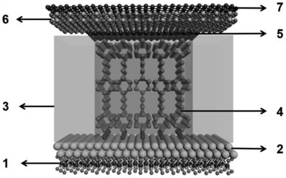
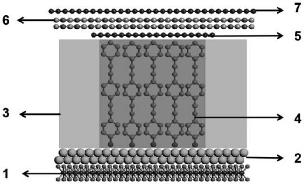
[0050] Example 1: Graphene drain / gate electrodes based on ultra-flat Au source electrodes and CVD growth, MoS 2 Vertical monomolecular film field effect transistor with template layer and h-BN insulating support layer / dielectric layer

[0051] 1. First, grow a large-area monolayer MoS on a silicon wafer by chemical vapor deposition (CVD) 2 film;

[0052] Then use an electron beam coater to coat the MoS 2 Evaporate 5-10nm gold film on the thin layer to obtain ultra-flat gold electrodes;

[0053] Then use CVD to grow single-layer h-BN (Nature, 2020, 579, 219) on the Cu(111) foil obtained by the annealing process, and repeat this step to obtain multiple single-layer (h-BN)-copper foils;

[0054] 2. Next, spin-coat PMMA glue on h-BN to form a PMMA-(h-BN)-copper foil sandwich structure;

[0055] 3. Then, put the structure into a 3% ammonium persulfate solution for etching. After the copper foil is dissolved, transfer the sample to clean deionized water to remove the residual am...

Embodiment 2

[0069] Example 2: Based on ultra-flat Au source electrode and mechanically exfoliated graphene drain / gate electrode, MoS 2 Vertical monomolecular film field effect transistor with template layer and h-BN insulating support layer / dielectric layer

[0070] 1. First, obtain one or few layers of MoS by mechanical exfoliation 2 , that is, repeated tearing with adhesive tape;

[0071] 2. Then, using polydimethylsiloxane (PDMS) as a transfer medium, the MoS 2 transferred to silicon substrates to obtain MoS 2 Template layer, used as a growth template for ultraflat gold films; specifically, MoS on tape contacted with polydimethylsiloxane (PDMS) on top of a glass slide 2 , when separated, MoS 2 A thin layer will remain on the PDMS. Tuning of MoS via a 3D translation stage in a microscope system 2 aligned with the silicon substrate. At this time, a slight force is applied to the glass slide, so that the MoS 2 Adhering to a silicon substrate, followed by slow detachment of PDMS, t...

Embodiment 3

[0084] Example 3: Graphene drain / gate electrodes based on ultra-flat Au source electrodes and CVD growth, WTe 2 Vertical monomolecular film field effect transistor with template layer and h-BN insulating support layer / dielectric layer

[0085] According to the steps of Example 1, only the MoS in the two-dimensional material template layer 2 Replaced by CVD grown WTe 2 The material obtains the graphene drain electrode / gate electrode based on ultra-flat Au source electrode and CVD growth provided by the present invention, WTe 2 Vertical monomolecular film field effect transistor with template layer and h-BN insulating support layer / dielectric layer.


PUM

PropertyMeasurementUnit
thicknessaaaaaaaaaa
thicknessaaaaaaaaaa
thicknessaaaaaaaaaa

Abstract

The invention discloses a vertical monomolecular film field effect transistor based on a two-dimensional laminated heterostructure and a preparation method of the vertical monomolecular film field effect transistor, and belongs to the field of new materials and molecular field effect transistors. The vertical monomolecular film field effect transistor is composed of the two-dimensional material template layer, the ultra-flat metal electrode, a two-dimensional material insulating support layer, a self-assembled monomolecular film, a two-dimensional material drain terminal electrode, an insulating two-dimensional material dielectric layer and a conductive two-dimensional material gate electrode layer. According to the invention, a novel two-dimensional material is adopted to replace the gridand dielectric layer materials in a traditional field effect transistor, a two-dimensional material insulating layer is introduced to accurately control the atomic-scale thickness of the electrode spacing, and the two-dimensional material thin layer is introduced to improve the flatness of the metal electrode, so that the device achieves the atomic-scale flatness and controllable atomic layer thickness; the vertical molecular field effect transistor which has room temperature stability, is regulated and controlled by the solid-state grid and is provided with the ultra-flat metal electrode isrealized, and the stability of the device and the possibility of large-scale integration are greatly improved.

Description

technical field [0001] The invention belongs to the field of new materials and molecular field effect transistors, in particular to a vertical monomolecular film field effect transistor using two-dimensional materials as ultra-flat metal electrode growth templates, insulating support layers, gate electrode layers, dielectric layers, and drain terminal electrodes. . Background technique [0002] Transistors are the core of electronic circuits in the traditional semiconductor industry. Since the first model of transistors was proposed in 1947, researchers have developed various forms of transistors. The basic principle is: by applying an appropriate voltage to the gate A gate electric field is generated in the dielectric layer to adjust the carrier concentration at the interface between the insulating layer and the semiconductor layer, so that the current between the source and drain electrodes can be adjusted. Therefore, on the one hand, the logic function of the switch can ...

Claims


Application Information

Patent Timeline
Patent Type & Authority Applications(China)
IPC IPC(8): H01L51/05H01L51/30H01L51/40
CPCH10K71/00H10K85/00H10K10/468H10K10/46H10K10/481
Inventor 贾传成李佩慧常新月郭雪峰
Owner NANKAI UNIV
Why Eureka
Try Eureka