An environmental electromagnetic field energy harvesting device and its preparation method
A technology of energy collection and electromagnetic field, which is applied in the field of micro-energy, can solve problems such as unexpected and interference, and achieve the effect of simple structure, good practicability, and easy working mode
- Summary
- Abstract
- Description
- Claims
- Application Information
AI Technical Summary
Problems solved by technology
Method used
Image
Examples
preparation example Construction
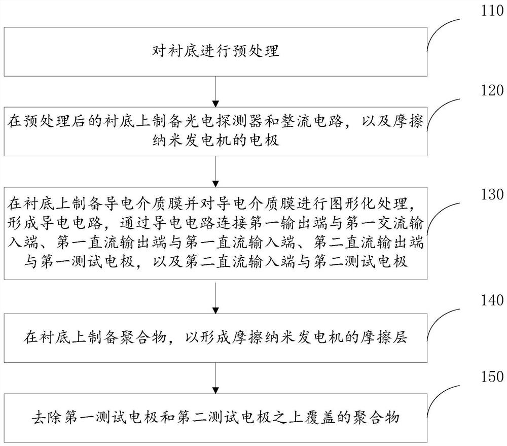
[0031] An embodiment of the present invention provides an environmental electromagnetic field energy harvesting device, including a receiving electrode, a rectifying circuit, and a first test electrode and a second test electrode prepared on the same substrate. Preferably, the rectification circuit is a bridge rectification circuit. The system can be obtained through the preparation method as described below, and its specific process steps are as follows: figure 1 shown, including:
[0032] Step 110, pretreating the substrate;
[0033] Specifically, the substrate was ultrasonically cleaned with acetone and isopropanol, and dried with high-purity nitrogen. Substrates used include: polyethylene terephthalate (PET), polyethylene naphthalate (PEN), polyimide (PI), polyvinyl chloride (PVC), polycarbonate (PC ), polystyrene (PS), polyethylene (PE), polypropylene (PP), sapphire (Al 2 o 3 ), silicon (Si), silicon carbide (SiC), quartz glass (SiO 2 ) or gallium arsenide (GaAs) ma...
Embodiment 1
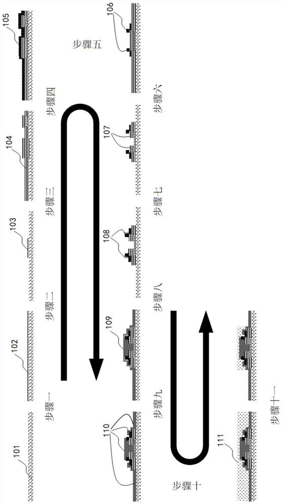
[0046] This embodiment provides a method for preparing an environmental electromagnetic field energy harvesting device, figure 2 It is a schematic diagram of the preparation process of the environmental electromagnetic field energy harvesting device provided in Embodiment 1 of the present invention.
[0047] Preparatory steps: prepare a 1000 micron thick quartz substrate 101, perform ultrasonic cleaning with acetone and isopropanol, and blow dry with high-purity nitrogen.
[0048] Step 1: sputtering a metal chromium (Cr) film 102 with a thickness of 50 nanometers on the upper surface of the quartz substrate 101 .
[0049] Step 2: Patterning the metal chromium film by using exposure technology and etching technology to form the chromium electrode 103 .
[0050] Step 3: Deposit 150 nanometer thick aluminum oxide (Al 2 o 3 ) insulating layer 104.
[0051] Step 4: sputtering a 40 nm zinc oxide film 105 on the aluminum oxide insulating layer 104 .
[0052] Step 5: Patterning ...
Embodiment 2
[0067] This embodiment provides a method for preparing an environmental electromagnetic field energy harvesting device, the difference from Embodiment 1 lies in step 12.
[0068] Step 12: Prepare a layer of polymethyl methacrylate (PMMA) on the surface of the ambient electromagnetic field energy harvesting device by spin-coating and heating-curing technology as the encapsulation layer of the rectifier circuit.
[0069] The environmental electromagnetic field energy harvesting device will generate a direct current output when the human body is in contact with the receiving electrode. The current output stabilizes at 10 until the human hand is removed -9 It is about ampere level, which is more than one order of magnitude higher than the noise current signal.
[0070] When the human body is in contact with the receiving electrode and is in contact with the active electronic device at the same time, the output current of the system can reach 10 -7 The ampere level is two orders ...
PUM
 Abstract
Description
Claims
Application Information


