Electroless palladium plating solution for wafer packaging field and preparation method thereof

A technology of wafer packaging and electroless plating, applied in liquid chemical plating, metal material coating process, coating, etc., can solve the problem of poor corrosion performance, ductility and bending performance, palladium plating deposition rate and dense palladium layer Uncontrollable corrosion resistance, instability of electroless palladium plating, etc., meet the requirements of good corrosion resistance test, meet the requirements of corrosion resistance test, and have excellent ductility

Active Publication Date: 2021-09-28
江苏矽智半导体科技有限公司
View PDF0 Cites 0 Cited by
  • Summary
  • Abstract
  • Description
  • Claims
  • Application Information

AI Technical Summary

Problems solved by technology

[0006] 1) If the plated parts are exposed to water or air for a long time, discoloration and oxidation will occur; this will easily affect the use of the plated parts in the later stage; and the palladium tank will be decomposed due to homogeneous catalysis during use. This causes the instability of electroless palladium plating
[0007] 2) Due to the difference in temperature and electroplating time in the electroless palladium plating layer, the deposition rate of palladium plating and the compactness of the palladium layer cannot be controlled, which eventually leads to poor corrosion performance, ductility and bending performance
In addition, water-soluble compounds are mainly used as palladium salts on the market at present, and their storage and transportation are in liquid state, which is not conducive to production operations

Method used


Image

  • Electroless palladium plating solution for wafer packaging field and preparation method thereof
  • Electroless palladium plating solution for wafer packaging field and preparation method thereof
  • Electroless palladium plating solution for wafer packaging field and preparation method thereof

Examples


preparation example Construction

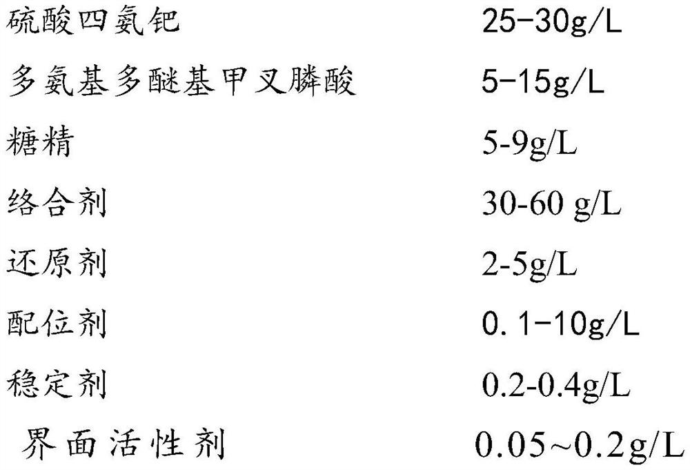
[0037] In order to achieve the above object, the present invention also provides a method for preparing an electroless palladium plating solution used in the field of wafer packaging, comprising the following specific steps:

[0038] 1) Prepare a palladium tank, and the palladium tank is equipped with a stirring pump;

[0039] 2) Pour tetraammine palladium sulfate into the palladium tank, then add deionized water and continuously stir until the tetraammine palladium sulfate is completely dissolved, and prepare solution A after the mass concentration of tetraammine palladium sulfate is 25-30g / L ;

[0040] 3) Add citric acid and malic acid with a concentration ratio of 6:1 to solution A in turn, and stir to obtain solution B;

[0041] 4) While continuing to stir solution B, add polyaminopolyether group methylene phosphonic acid with a concentration of 5-15g / L, saccharin with a concentration of 5-9g / L, a reducing agent with a concentration of 2-5g / L, Solution C is obtained afte...
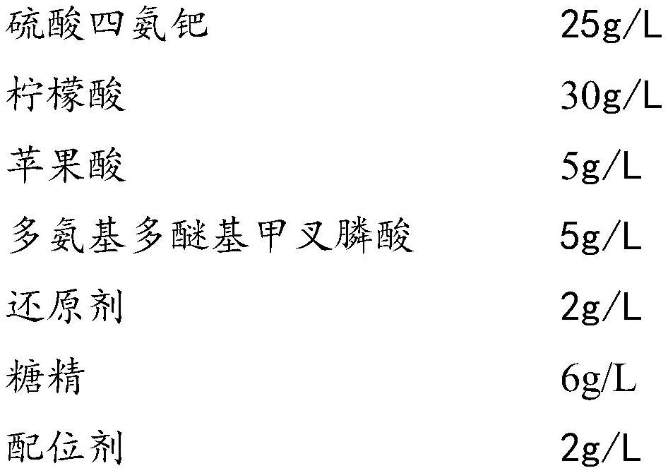
Embodiment 1

[0055]

[0056]

[0057] The bath temperature is 50°C; the time is 10 minutes.

[0058] Using the palladium plating solution in the present embodiment, the palladium layer appearance of the plated piece that obtains is flat and silvery white; Observing with a microscope, it can be clearly seen that the coating structure is very compact, and the coating crystallization is fine and uniform, without cracks; through 180 ° bending test test, The bonding strength of the coating is very good, and no obvious cracks are observed when magnified by 100 times.

Embodiment 2

[0060]

[0061] The bath temperature is 55°C; the time is 12 minutes.

[0062] Using the palladium plating solution in the present embodiment, the palladium layer appearance of the plated piece that obtains is flat and silvery white; Observing with a microscope, it can be clearly seen that the coating structure is very compact, and the coating crystallization is fine and uniform, without cracks; through 180 ° bending test test, The bonding strength of the coating is very good, and no obvious cracks are observed when magnified by 100 times.


PUM


Abstract

The invention discloses an electroless palladium plating solution used in the field of wafer packaging and a preparation method thereof, which comprises the following components in terms of mass concentration: 25-30 g / L of tetraammonia palladium sulfate; 30-30 g / L of complexing agent 60g / L; malic acid 5‑10g / L; polyamino polyether methylene phosphonic acid 5‑15g / L; saccharin 5‑9g / L; reducing agent 2‑55‑9g / L; complexing agent 0.1‑10g / L; Stabilizer 0.2-0.4g / L; Surfactant 0.05-0.2g / L. After mixing the above tetraammonium palladium sulfate, citric acid, malic acid, polyamino polyether methylene phosphonic acid, saccharin, complexing agent, stabilizer and surfactant according to the above ratio, use buffer to adjust the pH value to 6.5- After 8.5 minutes, a palladium plating solution is formed, and the preparation temperature is 50-60°C, and the palladium plating time is 5-15min. The coating structure obtained by using the palladium plating solution of the invention is very compact, and the coating crystallization is fine and uniform.

Description

technical field [0001] The invention relates to the technical field of packaging and materials, in particular to an electroless palladium plating solution used in the field of wafer packaging and a preparation method thereof. Background technique [0002] The general orientation of wafer-level packaging is to perform most or all of the packaging and testing procedures directly on the wafer, and then cut it into a single component. Wafer-level packaging has a smaller package size and better electrical performance. At present, it is mainly used in various semiconductor products, and its demand mainly comes from the requirements of portable products for light, thin and small features. [0003] There are very important surface treatment processes in wafer-level packaging, which are directly related to the use of subsequent electronic products. None of the existing surface treatment processes (nickel-gold, nickel-palladium-gold, palladium-gold, silver, tin, OSP, HASL) can simult...

Claims


Application Information

Patent Timeline
Patent Type & Authority Patents(China)
IPC IPC(8): C23C18/44
CPCC23C18/44
Inventor 洪学平姚吉豪
Owner 江苏矽智半导体科技有限公司
Why Eureka
Try Eureka