
Silicon carbide wafer one-way three-time two-way six-step cutting process

A cutting process and silicon carbide technology, which is applied in the direction of manufacturing tools, metal processing equipment, welding equipment, etc., can solve problems such as easy cracking, and achieve high yield, narrow kerf, and low cost effects

Active Publication Date: 2021-04-09
西安晟光硅研半导体科技有限公司
View PDF18 Cites 3 Cited by
  • Summary
  • Abstract
  • Description
  • Claims
  • Application Information

AI Technical Summary

Problems solved by technology

Machining is a common method in the past, but it is prone to cracking

Method used


Image

  • Silicon carbide wafer one-way three-time two-way six-step cutting process
  • Silicon carbide wafer one-way three-time two-way six-step cutting process
  • Silicon carbide wafer one-way three-time two-way six-step cutting process

Examples


Embodiment 1

[0031]Example 1: One-way three-dimensional six steps

[0032]Step 1: Modify existing clamping devices and turns to meet the processing of a sample of 150 mm diameter silicon carbide crystals;

[0033]Step 2:Figure 5 As shown, the sample is erected and held clamps;

[0034]Step 3: First of all, the experiment and select a larger, which can have a stable laser beam length of about 80-80mm, ensuring that the main shaft head remains the same height, the ability is 35mm (radius);

[0035]Step 4: From the symmetry position of the above thickness direction to the deepest position;

[0036]Step 5: Subsequently, the second / 3 times is then cut to the first same depth on the left and right, thereby establishing a relatively flat 3X water jet width, which is a second depth cut cut as a water column interference. The start surface;

[0037]Step 6: In the left side of the center symmetrical line, the same spout is used to cut to its deepest depth; note that this depth may be different from the first depth in the...


PUM

PropertyMeasurementUnit
diameteraaaaaaaaaa
thicknessaaaaaaaaaa
Mohs hardnessaaaaaaaaaa

Abstract

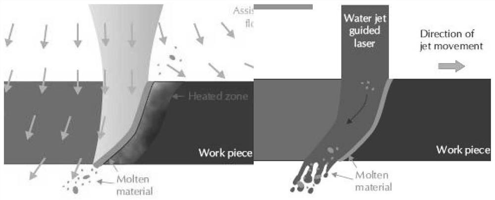
The invention discloses a method for cutting a silicon carbide wafer by stepped laser. The method comprises the following steps that firstly the silicon carbide wafer is cut to the deepest position at a symmetrical position in the thickness direction of a silicon carbide crystal ingot; then three times of cutting are conducted on the left side and the right side for the same depth as the first time, so that a relatively gentle face with multiple times of water jet widths is established, and the face serves as a starting face of second-depth cutting for avoiding water column interference; second-layer first cutting is carried out on the left side of the central symmetry line to the deepest depth by adopting a same nozzle; then secondary cutting is carried out on the right side of the thickness symmetry axis to reach the same depth as the first cutting of the second layer; and a third layer is cut for the first time to reach the depth above the radius of the silicon carbide crystal ingot. High-depth cutting of the single crystal silicon carbide crystal ingot is achieved through step method cutting, a SiC single crystal substrate is prepared in a high-efficiency, high-quality, low-cost, low-damage and high-yield mode, and the method has application and popularization value.

Description

Technical field[0001]The present invention relates to the field of silicon carbide wafer cutting processes, and more particularly to a silicon carbide wafer single-directional three-way hexahedral cutting process.Background technique[0002]SiC single crystal is a typical hardcod, which has a macquard hardness of 9.2 to 9.5, second only to diamond, which makes the processing and manufacturing process of SiC single crystal substrates more difficult. At present, the manufacturing process of the SiC single crystal substrate can be divided into cutting → rough research → fine research → polished several stages. Cutting as a primary critical process for manufacturing SiC single crystal substrates, the processing quality directly affects the material removal of subsequent steps, and finally processing quality (surface roughness and flatness), product productivity and processing cost, etc.. With the development of crystal growth and market demand, the demand for large diameter SiC single cry...

Claims


Application Information

Patent Timeline
Patent Type & Authority Applications(China)
IPC IPC(8): B23K26/38B23K26/402B23K26/70
CPCB23K26/38B23K26/402B23K26/702
Inventor 郭辉蒋树庆胡彦飞
Owner 西安晟光硅研半导体科技有限公司
Learn More