Sb-Si3N4 thin film material for phase change memory and preparation method thereof

A phase-change memory, sb-si3n4 technology, applied in the direction of electrical components, etc., can solve the problems of poor thermal stability of thin-film amorphous state, high power, high current of phase-change memory, etc.

Active Publication Date: 2021-05-11
NINGBO UNIV
View PDF6 Cites 0 Cited by
  • Summary
  • Abstract
  • Description
  • Claims
  • Application Information

AI Technical Summary

Problems solved by technology

However, the pure Sb film presents an explosive crystallization method, which leads to the poor thermal stability of the film in the amorphous state, and the crystallization temperature is low, only less than 65 ° C, w

Method used


Image

  • Sb-Si3N4 thin film material for phase change memory and preparation method thereof
  • Sb-Si3N4 thin film material for phase change memory and preparation method thereof
  • Sb-Si3N4 thin film material for phase change memory and preparation method thereof

Examples


preparation example Construction

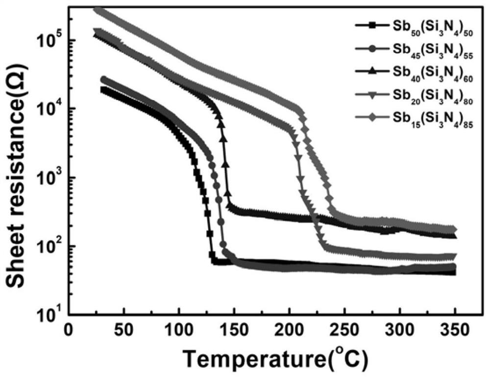
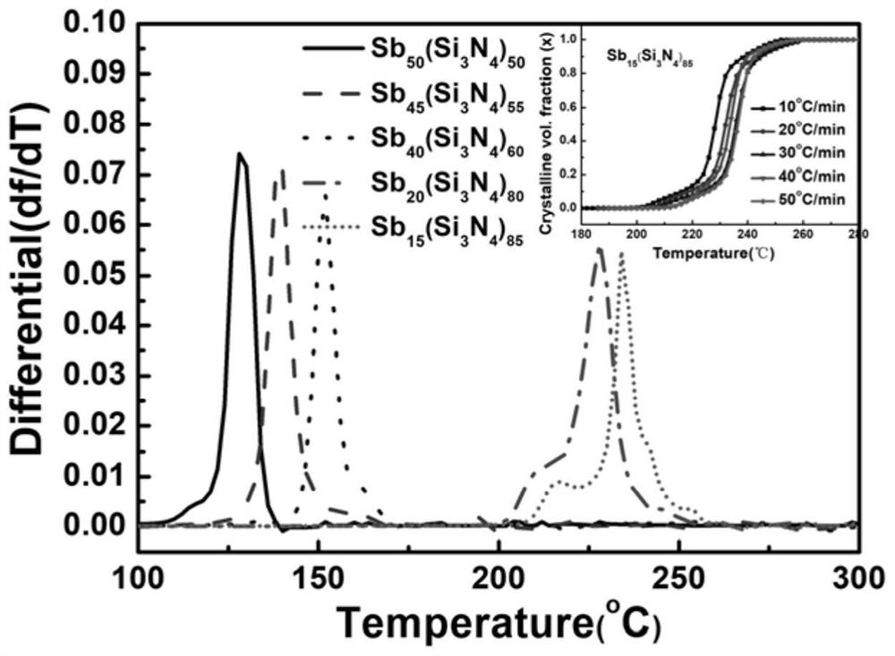
[0031] A kind of Sb-Si for phase change memory 3 N 4 Thin film material, its chemical structure is Sb x (Si 3 N 4 ) 100-x , where the atomic percentage of Sb is 15≤x≤50, the crystallization temperature of the material is between 110 and 210°C, and the amorphous resistance is 10 4 ~10 6 Ω, crystalline resistance 10 1 ~10 3 Ω. Its preparation method is: using high-purity round blocks of Sb and Si 3 N 4 The material is used as the target material, using a magnetron sputtering device, double targets are sputtered at the same time, high-purity argon is introduced as the working gas, and quartz wafers or silicon wafers are used as the substrate material for surface area deposition. The specific steps are as follows:

[0032] (1) Si 3 N 4 The round target and the back of the Sb round target are completely attached to a circular copper sheet with the same diameter as the target. The thickness of the copper sheet is about 1mm to obtain a magnetron sputtering coating target;...

Embodiment 1

[0038] A kind of Sb-Si for phase change memory 3 N 4 Thin film, its preparation method is as follows:

[0039] (1) Using Si 3 N 4 Simultaneous sputtering coating with Sb double target: Install the Sb target in the magnetron DC sputtering target, and the Si 3 N 4 The target is installed in the magnetron radio frequency sputtering target; vacuumize the sputtering chamber, when the vacuum degree in the sputtering chamber reaches 6×10 -4 Pa, fill the chamber with high-purity argon gas, the flow rate of argon gas is 50.0ml / min, until the initiation pressure required for sputtering is 0.3Pa in the chamber; turn on the radio frequency power supply, and after the initiation is stable, adjust the position where Sb is located. DC sputtering target power is 10W, Si 3 N 4 The magnetron radio frequency sputtering power where the target is located is 60W. After the power is stable, turn on the substrate turntable and set the rotation rate to 5rpm, open the baffle under the substrate,...

Embodiment 2

[0043] Same as Example 1, the difference is that the power of the DC sputtering target where the Sb is located is still 10W, and the Si 3 N 4 The RF power of the RF target is adjusted to 50W.

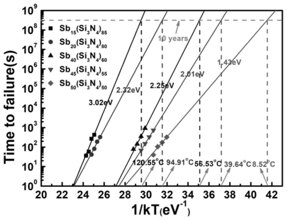
[0044] The Sb-Si prepared in above-mentioned embodiment 2 3 N 4 The film composition is measured by X-ray Energy Spectroscopy (EDS), and the film thickness is measured by a step meter. The test results are: the film composition is (Sb) 20 (Si 3 N 4 ) 80 , film thickness is 150nm. The corresponding crystallization temperature of the film is 200°C, and the amorphous resistance is 1.4×10 5 Ω, the crystalline resistance is 1×10 2 Ω; 10-year data retention temperature has been tested to be 94.91°C.


PUM

PropertyMeasurementUnit
Thicknessaaaaaaaaaa
Crystallization temperatureaaaaaaaaaa

Abstract

The invention discloses a Sb-Si3N4 thin film material for a phase change memory and a preparation method thereof. The Sb-Si3N4 thin film material is characterized in that the chemical structure of the Sb-Si3N4 thin film material is Sbx(Si3N4)100-x, and x is more than or equal to 15 and less than or equal to 50. The preparation method comprises the following steps: taking high-purity round blocks Si3N4 and Sb as target materials, introducing high-purity argon as working gas through a magnetron sputtering device by adopting a double-target co-sputtering method, taking a silicon wafer or a quartz plate as a substrate material, and carrying out surface deposition on the target materials; adjusting the Sb direct current sputtering power to be 10-20 W, adjusting the radio frequency power of the Si3N4 target to be 30-60 W and sputtering for 30 min at the room temperature, to obtain the Sb-Si3N4 thin film material. The Sb-Si3N4 thin film material has the advantages of high crystallization temperature, strong ten-year data retention, fast crystallization speed, good thermal stability and large amorphous and crystalline resistivity.

Description

technical field [0001] The invention relates to the field of phase-change memory materials, in particular to a kind of Sb-Si for phase-change memory 3 N 4 Thin film materials and methods for their preparation. Background technique [0002] Nowadays, the wide application of electronic products promotes the continuous development of memory. Compared with the flash memory in the current non-volatile memory market, phase change memory (PCM) not only solves the problem of low cycle times (~10 6 ) and long writing time (>10us), it also shows obvious advantages in terms of large capacity, high density, high speed, low power consumption, low cost, etc. PCM memory cells have been confirmed not to exist before the 5nm technology node any physical constraints. In addition, its low cost, simple manufacturing process, high storage density, low power consumption, strong data storage ability and many other advantages make phase change memory attract much attention and is considered t...

Claims


Application Information

Patent Timeline
IPC IPC(8): H01L45/00
CPCH10N70/8836H10N70/231H10N70/026H10N70/041
Inventor 吕业刚汪子洋廖立波
Owner NINGBO UNIV
Why Eureka
Try Eureka