Carbon-based multilayer film and preparation method and application thereof
A multi-layer thin-film, carbon-based technology, used in coatings, metal material coating processes, ion implantation plating, etc., can solve problems such as poor film/base bonding force, improve performance and life, and improve bonding. Effects of strength, good compatibility and metallurgy
- Summary
- Abstract
- Description
- Claims
- Application Information
AI Technical Summary
Problems solved by technology
Method used
Image
Examples
preparation example Construction
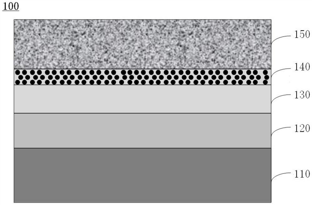
[0082] The preparation method of the above-mentioned carbon-based multilayer film is carried out by using an arc evaporation composite magnetron sputtering coating machine, and the arc evaporation composite magnetron sputtering coating machine is composed of a vacuum chamber, two magnetron sputtering sources, an electric arc The evaporation source is composed of a workpiece support that can rotate at the same time, and the workpiece support is installed inside the vacuum chamber. Among them, the two magnetron sources are equipped with pure Ta target and Ti target respectively, and the arc evaporation source is equipped with pure graphite target.
[0083] The invention also provides the application of the carbon-based multilayer film in the manufacture of electronic products.
[0084] Compared with the prior art, the carbon-based multilayer film of the present invention has the following beneficial effects:
[0085] The invention adopts Ta metal and Ti metal to form a double m...
Embodiment 1
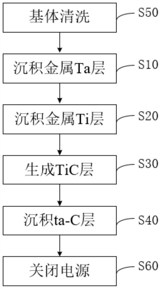
[0090] 1) Substrate cleaning: ultrasonically clean the silicon wafer substrate with alcohol, then rinse it with deionized water, dry it with dry compressed air, place the substrate on the workpiece support in the vacuum chamber, and evacuate the vacuum chamber to a vacuum degree of 1.0×10 –4 Below Pa. Turn on the ion source, pass 300 sccm of argon gas into the ion source, keep the strong pressure at 1Pa, set the ion source power to 1kW, set the workpiece support bias to -800V, and work for 30 minutes.
[0091] 2) Deposit metal Ta layer: Turn on the magnetron sputtering source equipped with Ta target, pass 150 sccm of argon gas into the vacuum chamber, and control the overall pressure of the vacuum chamber to 0.5Pa; at the same time, set the bias voltage of the substrate to -100V, and set the sputtering power supply to At 3kW, the deposition time was 10 minutes.
[0092] 3) Deposit metal Ti layer: turn on the magnetron sputtering source equipped with Ti target, pass 150 sccm o...
Embodiment 2
[0097] 1) Substrate cleaning: ultrasonically clean the silicon wafer substrate with alcohol, then rinse it with deionized water, dry it with dry compressed air, place the substrate on the workpiece support in the vacuum chamber, and evacuate the vacuum chamber to a vacuum degree of 1.0×10 –4 Below Pa. Turn on the ion source, feed 300 sccm of argon gas into the ion source, keep the strong pressure at 1Pa, set the ion source power to 1kW, set the workpiece support bias to -800V, and work for 30 minutes.
[0098] 2) Deposit metal Ta layer: Turn on the magnetron sputtering source equipped with Ta target, feed argon gas 180sccm into the vacuum chamber, and control the overall pressure of the vacuum chamber to 0.6Pa; at the same time, set the bias voltage of the substrate to -100V, and set the sputtering power supply to At 4kW, the deposition time was 8 minutes.
[0099] 3) Deposit metal Ti layer: Turn on the magnetron sputtering source equipped with Ti target, feed argon gas 180sc...
PUM
 Abstract
Description
Claims
Application Information


