A kind of preparation method of high-power far-infrared diamond laser single crystal composite material
A diamond single crystal and composite material technology, which is applied in the field of preparation of high-power far-infrared diamond laser single crystal composite materials, can solve the problems of poor thermal conductivity, multi-layer film structure multi-photon absorption, and affect the high power output of lasers, etc., to solve high heat problems, solving quantum deficit, and the effect of high output power
- Summary
- Abstract
- Description
- Claims
- Application Information
AI Technical Summary
Problems solved by technology
Method used
Image
Examples
Embodiment 1
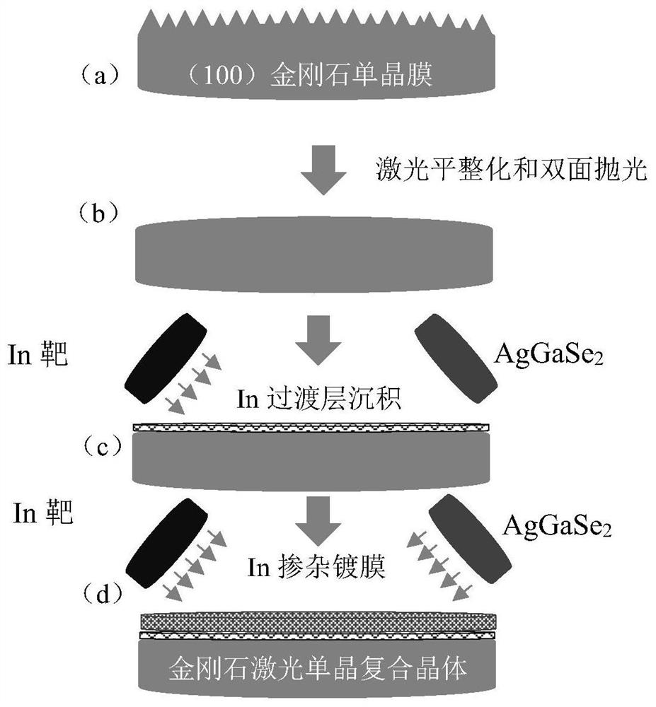
[0036] 1) A method for preparing a high-power far-infrared diamond laser single-crystal composite material, which mainly includes: preparing a high-quality, high-transmittance CVD (100) diamond single-crystal film, and using a microwave plasma chemical vapor deposition system (CVD) to deposit the diamond single-crystal film; The crystal film was grown at a controlled temperature of 900 °C, the growth rate was 6 μm / h, and the deposition time was 217 h. Finally, a 1.3 mm thick as-deposited (100) diamond single crystal film was obtained, such as figure 1 (a).
[0037] 2) Obtaining a double-sided polished diamond film, the specific steps include: firstly, performing laser planarization on the diamond growth surface, excising 0.3 mm thick diamond on the growth surface, removing large diamond particles on the surface, and then carrying out the diamond single crystal film on a single crystal polishing machine. For double-sided polishing, firstly adjust the rotating speed of the polis...
Embodiment 2
[0043] 1) A method for preparing a high-power far-infrared diamond laser single-crystal composite material, which mainly includes: preparing a high-quality, high-transmittance CVD (100) diamond single-crystal film, and using a microwave plasma chemical vapor deposition system (MPCVD) to deposit the diamond single-crystal film; The crystal film was grown at a controlled temperature of 950 °C, the growth rate was 7 μm / h, and the deposition time was 171 h. Finally, a deposited (100) oriented diamond single crystal film with a thickness of 1.2 mm was obtained, such as figure 1 (a).
[0044] 2) Obtaining a double-sided polished diamond film, the specific steps include: firstly, performing laser planarization on the diamond growth surface, excising 0.2 mm thick diamond on the growth surface, removing large diamond particles on the surface, and then performing the diamond single crystal film on a single crystal polishing machine. For double-sided polishing, firstly adjust the polishi...
PUM
| Property | Measurement | Unit |
|---|---|---|
| infrared transmittance | aaaaa | aaaaa |
| infrared transmittance | aaaaa | aaaaa |
Abstract
Description
Claims
Application Information

