Preparation method of silicon oxide fiber, and silicon oxide fiber

A technology of silicon oxide fiber and silicon oxide layer, which is used in semiconductor/solid-state device manufacturing, electrical components, circuits, etc., can solve the problem that the size and density of silicon oxide fibers are difficult to precisely control, the size of nanofibers is not uniform, and it is difficult to prepare Nanofibers and other issues, to achieve the effects of controllable density, good uniformity and controllable scale

Pending Publication Date: 2021-07-09
BEIJING NAURA MICROELECTRONICS EQUIP CO LTD
View PDF0 Cites 0 Cited by
  • Summary
  • Abstract
  • Description
  • Claims
  • Application Information

AI Technical Summary

Problems solved by technology

For another example, the hydrothermal method mixes silica sol and nitrate solution and disperses it ultrasonically, and then adds ethylenediamine after the nitrate solution dissolves, and stirs evenly to obtain a mixed solution; the mixed solution is transferred to a polytetrafluoroethylene-lined stainless steel In the reaction kettle, it is sealed and placed in a high-temperature oven for hydrothermal reaction, and then some post-processing steps are used to obtain silica fiber nano-products; this method uses a hydrothermal method, and the nucleation points will be uneven, so it is easy to cause subsequent The scale of the prepared nanofibers is not uniform
In addition, although the cost of preparing silica fibers by electrospinning is low, it is difficult to prepare nanofibers with uniform size.
It can be seen that the scale and density of silica fibers prepared by the preparation method of silica fibers in the related art are difficult to be accurately controlled, and there is still room for improvement in the uniformity of scale between batches during industrial production.

Method used


Image

  • Preparation method of silicon oxide fiber, and silicon oxide fiber
  • Preparation method of silicon oxide fiber, and silicon oxide fiber
  • Preparation method of silicon oxide fiber, and silicon oxide fiber

Examples


preparation example Construction

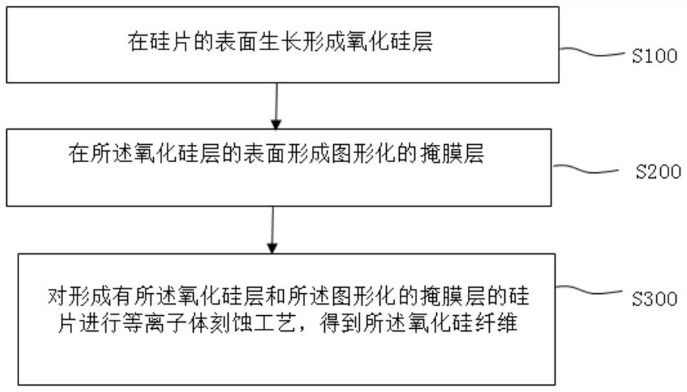
[0027] Such as figure 1 Shown, in some embodiments, a kind of preparation method of silica fiber is provided, comprising the following steps:

[0028] S100, growing and forming a silicon oxide layer on the surface of the silicon wafer;

[0029] S200, forming a patterned mask layer on the surface of the silicon oxide layer;

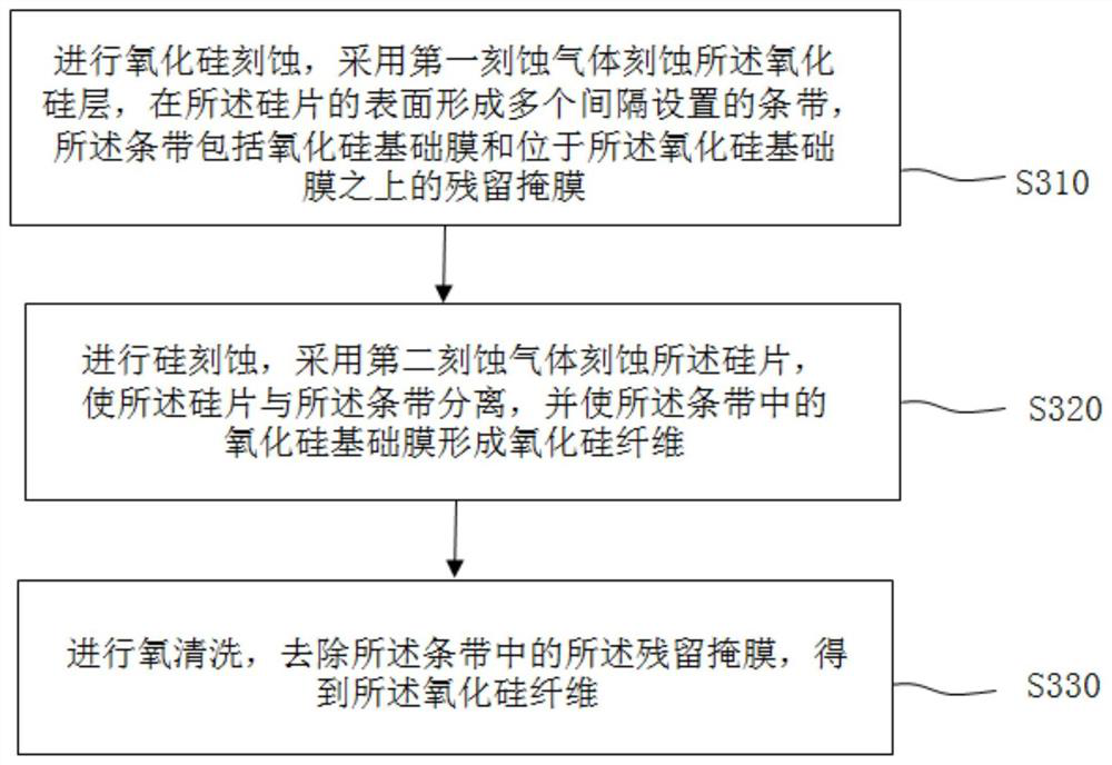
[0030] S300. Perform a plasma etching process on the silicon wafer formed with the silicon oxide layer and the patterned mask layer to obtain the silicon oxide fiber.

[0031] The preparation method of the silicon oxide fiber provided in the embodiment of the present application can be prepared by growing silicon oxide on a silicon wafer to form a silicon oxide layer, then photolithography to form a patterned mask layer, and then performing a plasma etching process to obtain an oxide fiber. Silicon fiber, in the process of plasma etching, the process parameters are adjusted according to the size of the required silicon oxide fiber, which is easy to opera...


PUM


Abstract

The invention discloses a preparation method of a silicon oxide fiber, and the silicon oxide fiber. The preparation method of the silicon oxide fiber comprises the following steps: allowing a silicon oxide layer to grow on the surface of a silicon wafer; forming a patterned mask layer on the surface of the silicon oxide layer; and performing a plasma etching process on the silicon wafer on which the silicon oxide layer and the patterned mask layer are formed to obtain the silicon oxide fiber. By adopting the preparation method of the silicon oxide fiber, the silicon oxide fiber with a uniform size can be prepared, and the prepared silicon oxide fiber is controllable in size, controllable in density and good in uniformity. Therefore, the problems that the scale and the density are difficult to accurately control, and the scale uniformity between batches is poor during industrial production in an existing method for preparing the silicon oxide fibers can be solved.

Description

technical field [0001] The application belongs to the technical field of semiconductor manufacturing, and in particular relates to a method for preparing silica fibers and the silica fibers. Background technique [0002] Oxygen and silicon are the two most abundant elements in the Earth's crust, and the compound silicon oxide, which consists of these two elements, is therefore a good candidate for cheap metamaterials. In addition to rich raw materials, silicon oxide also has the characteristics of insulation and hydrophobicity, and the prepared fiber materials are widely used in electrostatic suction filtration, self-cleaning and other fields. Due to the one-dimensional scale characteristics of the fiber material, it can also carry various functional nanoparticles, which further enriches the use of silica fibers. [0003] The methods for preparing silica fibers in the related art mainly include natural product extraction, hydrothermal method and electrospinning. For exampl...

Claims


Application Information

Patent Timeline
Patent Type & Authority Applications(China)
IPC IPC(8): H01L21/02H01L21/3065
CPCH01L21/0201H01L21/3065
Inventor 林源为张海苗
Owner BEIJING NAURA MICROELECTRONICS EQUIP CO LTD
Why Eureka
Try Eureka