Preparation method of embedded diamond-based silicon carbide composite substrate

A composite substrate and silicon carbide-based technology, which is applied in chemical instruments and methods, gaseous chemical plating, metal material coating technology, etc. Matching problems, to achieve the effect of solving heat concentration, reducing interface thermal resistance, and high thermal conductivity

Active Publication Date: 2021-07-23
UNIV OF SCI & TECH BEIJING +1
View PDF7 Cites 0 Cited by
  • Summary
  • Abstract
  • Description
  • Claims
  • Application Information

AI Technical Summary

Problems solved by technology

However, their combination is not simple and easy in actual operation, and there is still a problem of lattice mismatch between SiC and diamond.
Depositing diamond on a direct SiC surface, especially for substrates of two inches or larger, tends to be prone to cracking due to the internal stress of the film itself and the stress caused by material mismatch

Method used


Image

  • Preparation method of embedded diamond-based silicon carbide composite substrate

Examples


Embodiment 1

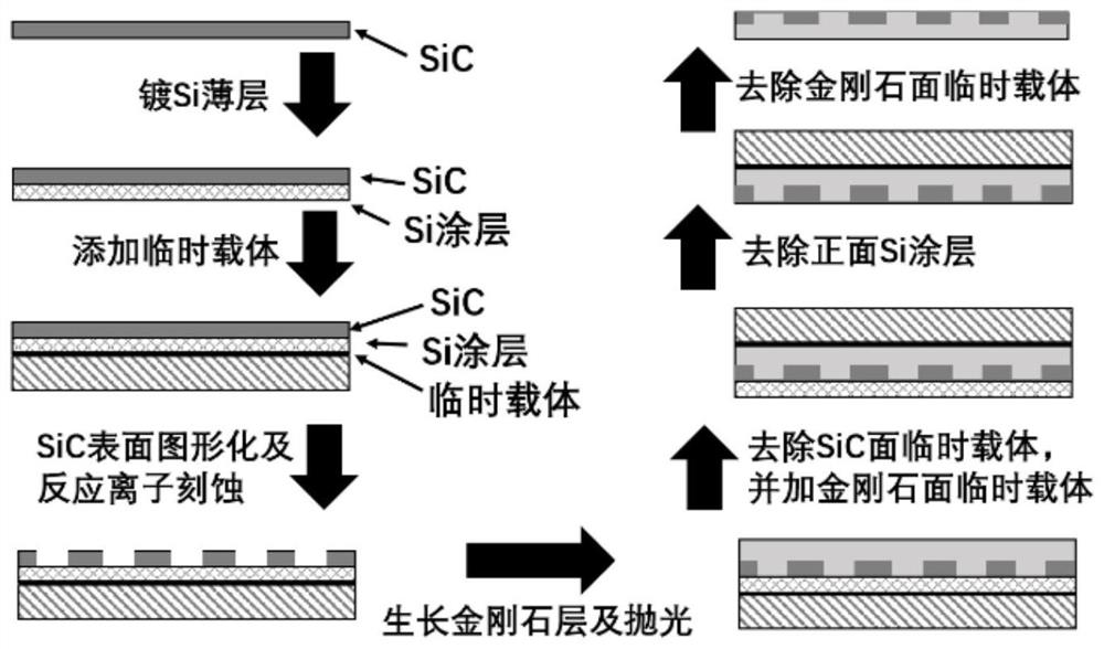
[0035] The magnetron sputtering technology was used to sputter for 0.5h under the conditions of power 100W, room temperature, chamber pressure 1Pa and self-bias voltage 300V, and a Si thin layer with a thickness of 200nm was plated. A high-temperature adhesive is coated on the Si thin layer, and the speed is maintained at 2000rpm for 6s. Attach a temporary carrier with exactly the same area as SiC on top of the thin Si layer. Afterwards, heat and cure in an oven, treat at 40°C for 2 hours, and then treat at 160°C for 2 hours. The SiC surface is patterned using mask and UV lithography, followed by CF 4 and O 2 Reactive ion etching is performed to remove the maskless SiC part and retain the SiC structure required by the design. Place the etched temporary carrier and SiC pattern in a microwave plasma vapor deposition system. Based on a two-inch substrate, the cavity pressure is 7.1kPa, the power is 4200W, and the deposition temperature is about 740°C, and CH is introduced int...

Embodiment 2

[0037] Magnetron sputtering technology was used under the conditions of power 400W, room temperature, chamber pressure 1Pa and self-bias voltage 200V for 5h, and a Si thin layer with a thickness of 2μm was deposited. Coat the high-temperature adhesive on the Si thin layer, and last 4s under the condition of rotating speed of 3000rpm. Attach a temporary carrier with exactly the same area as SiC on top of the thin Si layer. Afterwards, heat and cure in an oven, treat at 40°C for 2 hours, and then treat at 160°C for 2 hours. The SiC surface is patterned using mask and UV lithography, followed by CF 4 and O 2 Reactive ion etching is performed to remove the maskless SiC part and retain the SiC structure required by the design. Place the etched temporary carrier and SiC pattern in a microwave plasma vapor deposition system. Based on a two-inch substrate, the cavity pressure is 7.3kPa, the power is 4300W, and the deposition temperature is about 780°C, and CH is introduced into th...


PUM


Abstract

The invention relates to a preparation method of an embedded diamond-based silicon carbide composite substrate, and belongs to the field of semiconductor material preparation. The method comprises the following steps: firstly, adhering a temporary carrier to a silicon carbide (SiC) substrate plated with a Si coating, and then carrying out surface patterning and reactive ion etching on SiC to form a SiC layer with a pattern structure; and then depositing a layer of diamond on the surface to cover SiC, and grinding and polishing the surface of the diamond layer. Then, after the temporary carrier of the SiC substrate is removed, adhering the temporary carrier to the diamond side. After the original Si coating is removed through reactive ion etching, the temporary carrier on the diamond side is removed, and finally the embedded diamond-based SiC composite substrate is obtained. Heat can be quickly dissipated under the conditions of high power and high integration, meanwhile, the excellent performance of SiC and diamond serving as wide bandgap semiconductors can be fully played, and a preparation basis for the structural design of a wide bandgap semiconductor heterogeneous material is provided.

Description

Technical field [0001] The invention belongs to the field of semiconductor material preparation. Its characteristic is that it can make full use of the excellent properties of SiC and diamond to prepare embedded diamond-based SiC composite substrates, thereby providing a substrate foundation for subsequent circuit design and device packaging. First, a temporary carrier is adhered to the SiC substrate plated with Si coating, and then the SiC is surface patterned and reactive ion etched to form a SiC layer with a patterned structure. Then a layer of diamond is deposited on the surface to cover the SiC, and the surface of the diamond layer is ground and polished. Subsequently, after removing the temporary carrier of the SiC substrate, the temporary carrier is adhered to the diamond side. After removing the original Si coating through reactive ion etching, the temporary carrier on the diamond side is removed, and finally an embedded diamond-based SiC composite substrate is obtai...

Claims


Application Information

Patent Timeline
IPC IPC(8): C30B25/18C30B25/04C30B25/14C30B29/04C23C16/01C23C16/02C23C16/04C23C16/27C23C16/50
CPCC23C16/01C23C16/0272C23C16/042C23C16/27C23C16/50C30B25/04C30B25/14C30B25/183C30B25/186C30B29/04
Inventor 郑宇亭李成明张钦睿刘思彤魏俊俊刘金龙陈良贤欧阳晓平
Owner UNIV OF SCI & TECH BEIJING
Why Eureka
Try Eureka