A kind of method and semiconductor that carry out p-type doping to tmdcs based on ptfe

A PTFE, p-type technology, applied in semiconductor devices, semiconductor/solid-state device manufacturing, electrical components, etc., can solve the problems of volatile doping and low efficiency

Active Publication Date: 2022-05-03
FUDAN UNIV
View PDF12 Cites 0 Cited by
  • Summary
  • Abstract
  • Description
  • Claims
  • Application Information

AI Technical Summary

Problems solved by technology

[0007] Aiming at the problem of low efficiency and volatile doping of two-dimensional transition metal chalcogenides after the p-type doping of two-dimensional transition metal chalcogenides by fluorine-containing small molecules in the prior art, the purpose of the present invention is to provide a PTFE-based doping Method and semiconductor for p-type doping of TMDCs

Method used


Image

  • A kind of method and semiconductor that carry out p-type doping to tmdcs based on ptfe
  • A kind of method and semiconductor that carry out p-type doping to tmdcs based on ptfe
  • A kind of method and semiconductor that carry out p-type doping to tmdcs based on ptfe

Examples


Embodiment 1

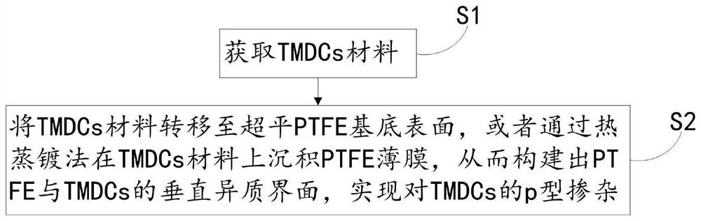
[0046] A method for p-type doping of TMDCs (two-dimensional transition metal dichalcogenides) based on PTFE (polytetrafluoroethylene), such as figure 1 As shown, step S1 and step S2 are included.

[0047] Step S1, obtaining TMDCs materials.

[0048] Among them, the representative structure of TMDCs material is MXn. Wherein, M is a metal, and the metal includes Mo, W, Pt, Hf, In, Re, Nb, Ta, Ga, Sn, Mn, Co, Zr and alloy compounds thereof. X includes O, S, Se, Te and their alloys [alloys here refer to compounds composed of chalcogen elements, such as MoSxSey, WSxTey, MoxWyS2, etc., such compounds are called alloy in English (Zhou, J., Lin, J ., Huang, X.et al.A library of atomically thin metalchalcogenides.Nature 556,355-359(2018), alloy is the meaning of alloy.] and Janus compound (Janus compound refers to replacing the chalcogen atoms in one layer with Another chalcogen atom belongs to TMDCs material structurally). Where n is a natural number greater than or equal to 1. In ...

Embodiment 2

[0066] The difference between it and Embodiment 1 is that the ultra-flat PTFE substrate configured in this embodiment is a PTFE sheet with a surface roughness of 5-7.5nm or a PTFE film with a surface roughness of 3.5-6.5nm, corresponding to:

[0067] 1. When the ultra-flat PTFE substrate is a PTFE sheet with a surface roughness of 5-7.5nm, it can be obtained by softening and reshaping the commercial PTFE sheet by hot pressing. The specific steps include:

[0068] First clamp and fix the commercial PTFE sheet between two ultra-flat carriers, the ultra-flat carrier is the same as Example 1, the difference lies in its SiO 2 Layer thickness is 200-300nm, surface roughness is 0.5-0.8nm;

[0069] Then, under the conditions of softening temperature of 280-320°C and softening time of 20-40min, the commercial PTFE sheet is softened and reshaped by hot pressing to obtain a PTFE sheet with a surface roughness of 5-7.5nm.

[0070] 2. When the ultra-flat PTFE substrate is a PTFE film with...

Embodiment 3

[0075] It differs from Embodiment 1 or 2 in that: before constructing the vertical heterogeneous interface between PTFE and TMDCs, it is also necessary to place the ultra-flat PTFE substrate in plasma for plasma treatment, thereby regulating the fluorine-containing surface layer of the ultra-flat PTFE substrate. quantity.

[0076] Specifically, in this embodiment, the plasma is set to be hydrogen or nitrogen, the flow rate is 1-2000 sccm, the plasma power is 1-5000 W, and the reaction time is 1-120 min.

[0077] For example, the PTFE sheet or PTFE film obtained in the above-mentioned embodiment one is placed in a hydrogen or nitrogen atmosphere with a gas flow rate of 1 sccm for plasma treatment, the plasma power is 10W, and the treatment time is 5min to regulate the PTFE sheet or PTFE film The fluorine content of the surface layer. Those skilled in the art can understand that the above-mentioned flow rate, power and reaction time will vary according to the different requirem...


PUM

PropertyMeasurementUnit
surface roughnessaaaaaaaaaa
softening pointaaaaaaaaaa

Abstract

The invention discloses a method and semiconductor for p-type doping of TMDCs based on PTFE, belonging to the technical field of advanced semiconductor devices. The method is as follows: transferring TMDCs material to a fluorine-containing ultra-flat PTFE substrate, thereby constructing a TMDs And the vertical heterointerface of PTFE, the interface has efficient hole doping regulation for TMDCs, by measuring the spectral structure and fluorescence lifetime of the transferred TMDCs, and characterizing the change of its energy band structure, it can be determined to realize the p-type of TMDCs Doping to obtain p-type doped TMDCs semiconductors, thus expanding the application in optoelectronic or electronic devices. The invention realizes the conversion of two-dimensional TMDCs from n-type to p-type doping at room temperature, and the adjustment effect is long-term, stable and suitable for large-scale production requirements. The method is easy to operate and has single atomic layer controllable doping accuracy. The strong electronegativity effect of fluorine compounds realizes the hole-doping type of 2D TMDCs.

Description

technical field [0001] The invention relates to the technical field of optoelectronic devices, in particular to a method for p-doping TMDCs based on PTFE and a semiconductor. Background technique [0002] Two-dimensional transition metal dichalcogenides (TMDCs) have demonstrated great potential as next-generation compound semiconductors beyond the competition of Moore's Law. They are rich in combinations, and have different crystal phases and crystal structures, thicknesses, and different stacking methods. The most important thing is that they have continuously adjustable band gaps from metal phases to semiconductor phases. However, 2D transition metal chalcogenides tend to have typical n-type semiconducting properties due to thermodynamic defects in their crystal structures (such as sulfur defects, etc.). [0003] Unlike silicon-based materials with mature n-type and p-type doping, the preparation process of p-doped two-dimensional transition metal chalcogenides has not be...

Claims


Application Information

Patent Timeline
Patent Type & Authority Patents(China)
IPC IPC(8): H01L21/385H01L21/02H01L29/24
CPCH01L21/385H01L29/24H01L21/02568
Inventor 孙正宗刘瀚祺巴坤
Owner FUDAN UNIV
Why Eureka
Try Eureka