High-temperature anti-oxidation ultrathin heating film and preparation method thereof
A high-temperature anti-oxidation and heating film technology, which is applied to heating element materials, ohmic resistance heating, electric heating devices, etc., can solve problems such as inconsistent thermal expansion coefficients, shedding, and complicated manufacturing processes, so as to avoid warping due to heating, increase geometric dimensions, The effect of simple preparation method
- Summary
- Abstract
- Description
- Claims
- Application Information
AI Technical Summary
Problems solved by technology
Method used
Image
Examples
Embodiment 1
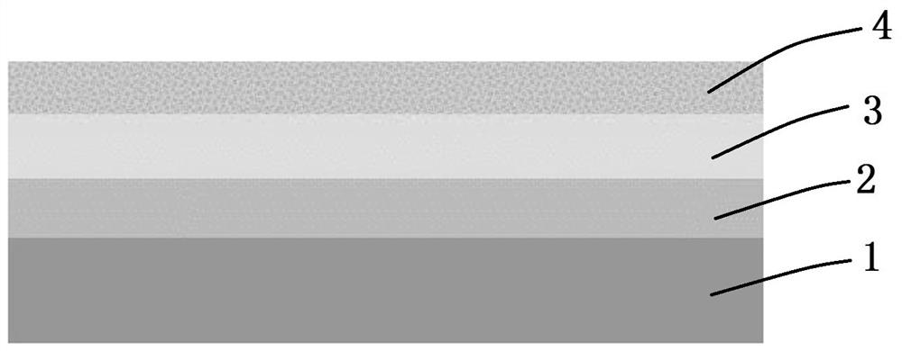
[0037] A high-temperature anti-oxidation ultra-thin heating film, such as figure 1 As shown, it includes an insulating base layer 1 , a conductive layer 2 , a transition layer 3 and an oxide layer 4 in sequence.
[0038] It is prepared by the following steps:
[0039] S1. Use a ceramic sheet with a thickness of 100 μm as the insulating base layer, use magnetron sputtering technology, use the Cu target as the sputtering source material, deposit 60 minutes, and then plate a layer of Cu with a thickness of 5 μm on the insulating base layer. layer.
[0040] S2. Use magnetron sputtering technology, use Cr target as the sputtering source material, pass in a low oxygen flow rate of 1 mL / min, so that Cr is not completely oxidized, and the deposition time is 15 minutes, and a layer can be coated on the conductive layer An oxide film of Cr with a thickness of 1 μm serves as a transition layer.
[0041] Cr cannot be completely oxidized to Cr due to insufficient oxygen intake 2 o 3 ,...
Embodiment 2
[0046] A high-temperature anti-oxidation ultra-thin heating film sequentially includes an insulating base layer, a conductive layer, a transition layer and an oxide layer.
[0047] It is prepared by the following steps:
[0048] S1. Use a stainless steel sheet with a thickness of 150 μm as the insulating base layer, use magnetron sputtering technology, use the Ag target as the sputtering source material, deposit 60 min, and plate a layer of Ag with a thickness of 6 μm on the insulating base layer as a conductive layer.
[0049] S2. Use magnetron sputtering technology, use Cr target as the sputtering source material, pass in a low oxygen flow rate of 1 mL / min, so that Cr is not completely oxidized, and the deposition time is 25 minutes, and a layer can be coated on the conductive layer An oxide film of Cr with a thickness of 1.2 μm serves as a transition layer. . Cr cannot be completely oxidized to Cr due to insufficient oxygen intake 2 o 3 , the metal oxide in the transiti...
Embodiment 3
[0054] A high-temperature anti-oxidation ultra-thin heating film sequentially includes an insulating base layer, a conductive layer, a transition layer and an oxide layer.
[0055] Prepared by the following steps:
[0056] S1. Using a PI film with a thickness of 80 μm as the insulating base layer, using magnetron sputtering technology, using the Ag target as the sputtering source material, depositing for 300 min, and plating a layer of Ag with a thickness of 50 μm on the insulating base layer as a conductive layer.
[0057] S2. Using the magnetron sputtering technology, using the Si target as the sputtering source material, injecting a lower flow rate of oxygen at 2 mL / min, the deposition time is 50 minutes, and coating a layer of Si oxide with a thickness of 5 μm on the conductive layer membrane, as a transition layer. Si cannot be completely oxidized to SiO due to insufficient oxygen influx 2 , the metal oxide in the transition layer is SiO x , 0<x<2.
[0058] S3. Using ...
PUM
| Property | Measurement | Unit |
|---|---|---|
| thickness | aaaaa | aaaaa |
| thickness | aaaaa | aaaaa |
| thickness | aaaaa | aaaaa |
Abstract
Description
Claims
Application Information


