

Nitrogen-doped P-type monocrystalline silicon manufacturing method
A manufacturing method, single crystal silicon technology, applied in the direction of single crystal growth, single crystal growth, chemical instruments and methods, etc., can solve the problem of easy boron simple substance volatilization, uncontrollable oxygen precipitation, affecting gettering effect, P-type silicon wafer quality, etc. question
- Summary
- Abstract
- Description
- Claims
- Application Information
AI Technical Summary
Problems solved by technology
Method used
Image

Examples
Embodiment Construction
[0026] The technical solutions in the embodiments of the present invention will be clearly and completely described below.
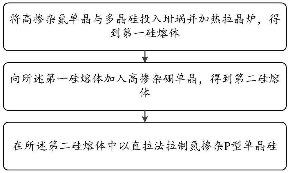
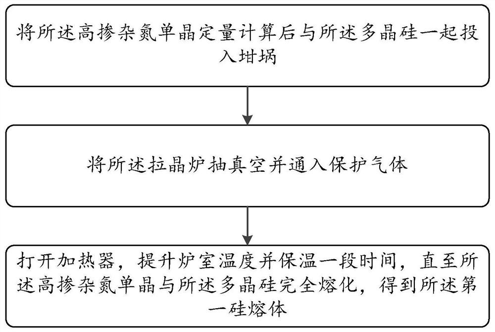
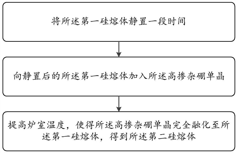
[0027] The nitrogen-doped P-type single-crystal silicon manufacturing method of the present invention is based on the Czochralski method, and at the same time cooperates with the solid-phase doping method to prepare nitrogen-doped P-type single-crystal silicon. That is, polysilicon and dopants are placed together in a crucible and heated to form a melt, and the melt is pulled to grow into single crystal silicon. In the present invention, a highly doped nitrogen single crystal and polycrystalline silicon are put into a crucible and heated in a crystal pulling furnace to obtain a first silicon melt; a highly doped boron single crystal is added to the first silicon melt to obtain a second silicon melt Body; Nitrogen-doped P-type single crystal silicon is pulled by Czochralski method in the second silicon melt.
[0028] In order to reduce the technical prob...
PUM
 Abstract
Description
Claims
Application Information