Electron transport ink, electron transport film, electroluminescent diode and display device

An electron transport and electron transport material technology, applied in the field of electronic display, can solve the problems of device leakage current, poor electron transport layer performance, and quantum dot light-emitting diode luminous performance and life performance decline.

Active Publication Date: 2022-02-11
GUANGDONG JUHUA PRINTING DISPLAY TECH CO LTD
View PDF5 Cites 0 Cited by
  • Summary
  • Abstract
  • Description
  • Claims
  • Application Information

AI Technical Summary

Problems solved by technology

[0004] However, compared with electron transport layers prepared by magnetron sputtering and chemical vapor deposition, the performance of electron transport layers prepared by solution methods such as inkjet printing is remarkable poor
Specifically, when such an electron transport layer is applied in a quantum dot light-emitting diode, the device will generate leakage current
Moreover, in

Method used


Image

  • Electron transport ink, electron transport film, electroluminescent diode and display device
  • Electron transport ink, electron transport film, electroluminescent diode and display device

Examples


preparation example Construction

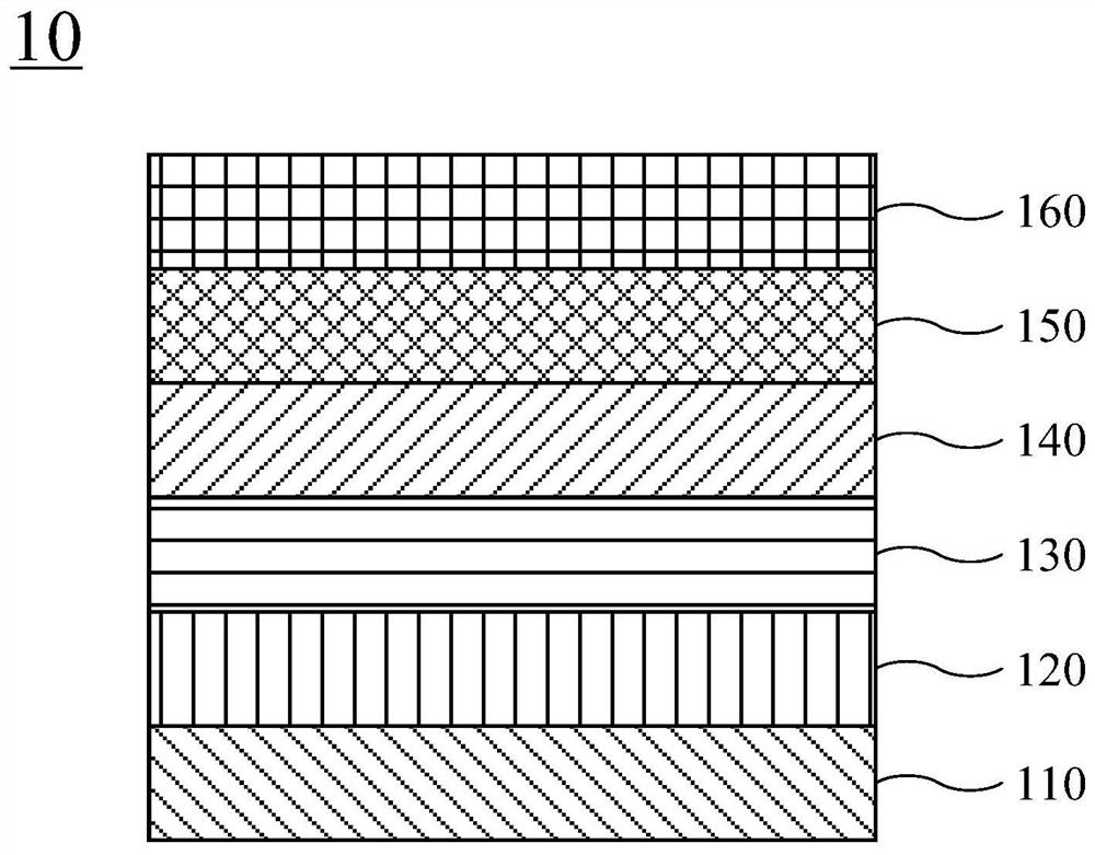
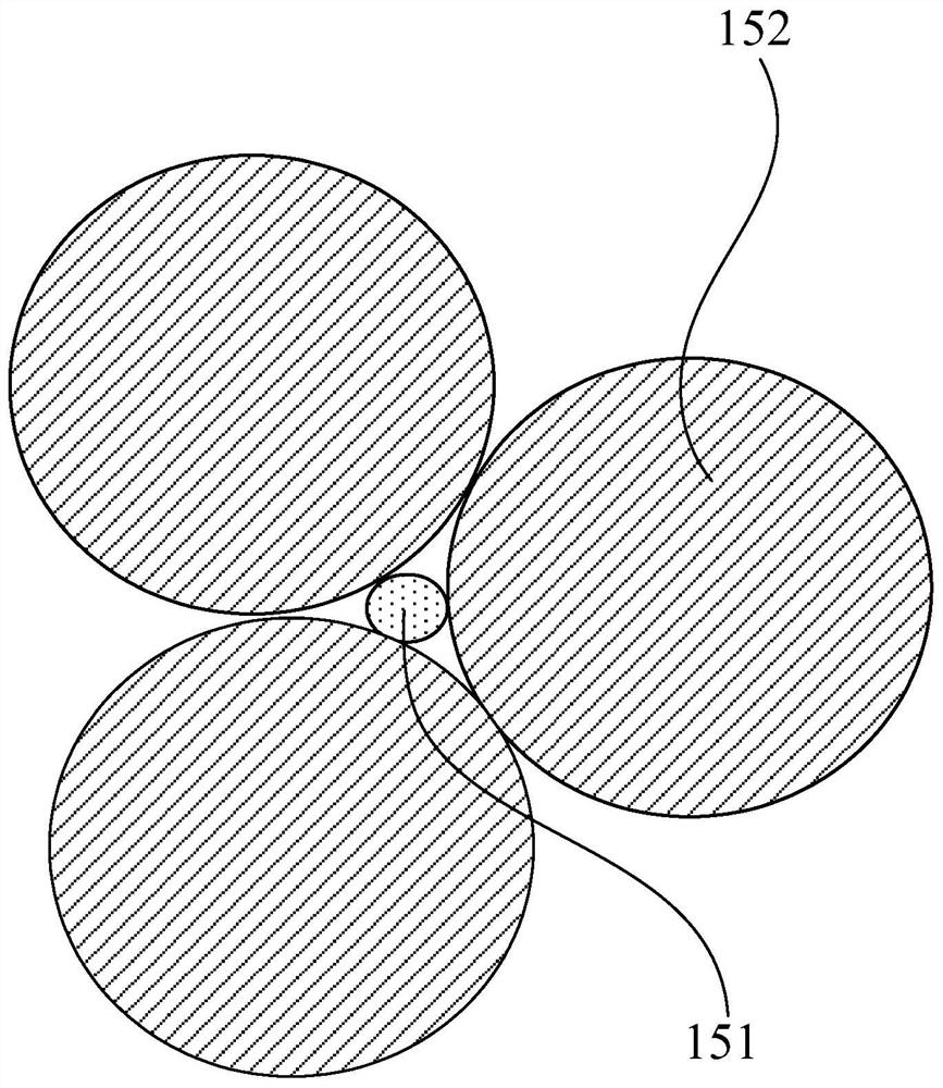
[0050] In the electroluminescent diode 10, the electron transport layer 150 is a thin film formed by stacking two types of nanoparticles with different particle sizes. The thin film may be formed by removing the dispersant in the ink including the two kinds of nanoparticles with different particle sizes after being formed on the surface of the light-emitting layer 140 . Specifically, the preparation method of the electron transport layer may include the following steps:

[0051] The ink is formed on the base material by a solution method, and then the dispersant in the ink is removed by heating and drying, and at the same time, the nano-material thin film is annealed. Annealing treatment can reduce the overall free energy of the film to a certain extent, reconstruct the crystal structure of the nanomaterials, eliminate some defects in the nanomaterials, and make the nanomaterials bond more closely, improving the electrical properties of the film.

[0052] Among them, the solu...

Embodiment 1

[0070] Under stirring, 1 g of ZnO spherical nanoparticles with a particle size of about 20 nm, 0.01 g of ZnO spherical nanoparticles with a particle size of about 3 nm, 50 g of glycerol, and 10 g of isopropanol solvent were added to a 100 mL round bottom flask. , and continue to stir the mixture for 30 minutes to make it disperse uniformly without coagulation to obtain ZnO ink.

Embodiment 2

[0072] Under stirring, 1 g of ZnMgO spherical nanoparticles with a particle size of about 30 nm, 0.02 g of ZnMgO nanoparticles with a particle size of about 4 nm, 50 g of glycerol, and 10 g of isopropanol solvent were added to a 100 mL round-bottomed flask in turn, The mixture was continued to be stirred for 30 minutes to make it dispersed uniformly without coagulation to obtain ZnMgO ink.


PUM

PropertyMeasurementUnit
Particle sizeaaaaaaaaaa
Thicknessaaaaaaaaaa
Thicknessaaaaaaaaaa

Abstract

The invention discloses electron transport ink, an electron transport layer, an electroluminescent diode and a display device. The electron transmission ink comprises a dispersing agent and dispersoid dispersed in the dispersing agent, the dispersoid comprises a first electron transmission material and a second electron transmission material, the first electron transmission material and the second electron transmission material are both selected from nano particles of materials with electron transmission capacity, the particle size of the second electron transmission material is 20-100 nm, and the particle size ratio of the first electron transport material to the second electron transport material is (0.05-0.15): 1. An electron transmission film prepared from the electron transmission ink is more compact, generation of leakage current can be effectively inhibited, and the current efficiency of a device is improved. In addition, the electron transport film can also play a role in balancing carriers in the electroluminescent diode, and the luminous efficiency of the device is improved.

Description

technical field [0001] The invention relates to the technical field of electronic display, in particular to an electronic transmission ink, an electronic transmission film, an electroluminescent diode and a display device. Background technique [0002] Electroluminescent diode devices are widely used in display devices. Among them, organic light emitting diodes and quantum dot light emitting diodes have the advantages of high color gamut, self-luminescence, low startup voltage and fast response speed, and are considered to be the most promising electroluminescent devices. Light-emitting diodes have received extensive attention and research. [0003] Conventional multilayer electroluminescent diode device structures generally include a cathode, an electron transport layer, an emissive layer, a hole transport layer and an anode. The layers can be prepared by, for example, magnetron sputtering, chemical vapor deposition, and the like. But these methods have some shortcomings....

Claims


Application Information

Patent Timeline
IPC IPC(8): H01L51/50H01L51/56
CPCH10K71/135H10K71/15H10K50/115H10K50/165
Inventor 罗健庄锦勇
Owner GUANGDONG JUHUA PRINTING DISPLAY TECH CO LTD
Why Eureka
Try Eureka