Etching liquid activating agent as well as preparation method and application thereof

A technology of activator and etching solution, which is applied in the field of etching solution activator and its preparation, can solve the problems of affecting the production capacity of equipment, consuming a large amount of silicon wafers, and high cost, so as to improve equipment production capacity, speed up reaction and reduce activation cost effect

Pending Publication Date: 2022-03-15
JA SOLAR
View PDF0 Cites 0 Cited by
  • Summary
  • Abstract
  • Description
  • Claims
  • Application Information

AI Technical Summary

Problems solved by technology

[0004] This activation method needs to consume 4000-8000 silicon wafers each time to activate the etching solution, and it takes 1.5-2.5 hours. The large amount of silicon wafers consumed leads to high costs, and the long time consumption seriously affects the equipment production capacity.

Method used


Image

  • Etching liquid activating agent as well as preparation method and application thereof
  • Etching liquid activating agent as well as preparation method and application thereof
  • Etching liquid activating agent as well as preparation method and application thereof

Examples


preparation example Construction

[0043] The embodiment of the present invention also provides a preparation method of an etching solution activator, the preparation method comprising:

[0044] S01, dissolving surfactant, catalyst and dispersant in water to obtain a mixed solution.

[0045] Specifically, the surfactant, catalyst and dispersant are added to water, stirred and ultrasonically treated to uniformly dissolve the surfactant, catalyst and dispersant in the water. Wherein, the water is deionized water, and the temperature of the deionized water may be 65° C. during dissolution.

[0046] Optionally, the ultrasonic treatment conditions are: ultrasonic power 3000W, frequency 20KHz, temperature 40°C, ultrasonic duration 40min.

[0047] S02, adding silicon powder into the mixed solution to obtain an activator for etching solution for crystalline silicon solar cells.

[0048] In the preparation method of the etching solution activator provided in the embodiment of the present invention, a mixed solution ca...
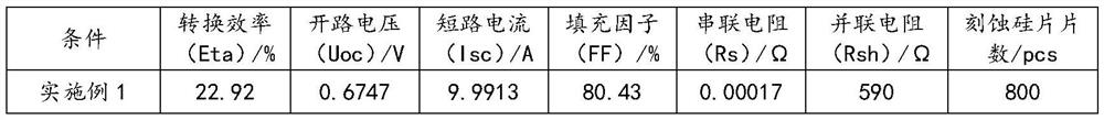
Embodiment 1

[0052] Embodiment 1: This embodiment provides a production method of a monocrystalline silicon solar cell, the production method comprising:

[0053] S11. Texturing treatment.

[0054] Specifically, the surface of the monocrystalline silicon wafer is textured with an alkaline solution. The alkali solution may be NaOH solution with a mass concentration of 2.1%. A trough-type texturing machine can be used to perform texturing reaction on silicon wafers for 420 seconds at a temperature of 82°C and a mass concentration of NaOH of 2.1% to obtain a textured surface.

[0055] S12. Diffusion treatment.

[0056] Specifically, a tube-type diffusion furnace is used to perform diffusion treatment on the silicon wafer under the conditions of a temperature of 850° C., a negative pressure of 100 mBar, and a nitrogen flow rate of 1000 sccm / min to form a PN junction.

[0057] S13. Laser doping treatment.

[0058] Laser is used for local heavy doping to reduce the contact resistance at the ...
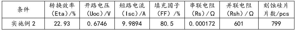
Embodiment 2

[0069] Embodiment 2: This embodiment provides a method for producing a monocrystalline silicon solar cell, the difference from Embodiment 1 is:

[0070] In this embodiment, the mixed solution is composed of dimethyl dodecyl amine oxide, palladium acetate, tri-tert-butylphosphine tetrafluoroborate and water, and the mixed solution includes each component in mass percentage: 10% dimethyl deca Dialkylamine oxide, 4% palladium acetate, 6% tri-tert-butylphosphine tetrafluoroborate, and 80% deionized water.

[0071] The etching solution activator in Example 2 can quickly activate the etching solution in the wet etching etch tank, shorten the activation time, and do not need to use a large number of silicon wafers to run the film to activate the etching solution. It can be directly produced after activating the etching solution, and the initial quality A 10g silicon wafer loses 0.30g in weight after etching, the reflectivity after back etching is 27.30%, and the conversion efficiency...


PUM


Abstract

The invention discloses an etchant activator and a preparation method and application thereof, the etchant activator is used for manufacturing crystalline silicon solar cells, the etchant activator comprises silicon powder and a mixed solution, and the mixed solution comprises a surfactant, a catalyst, a dispersant and water. When the activating agent is used, the activating agent is added into the etching liquid for the crystalline silicon solar cell, so that the etching liquid can be quickly activated, the activation time is shortened to 15-20 minutes, the productivity of equipment is favorably improved, the consumption of silicon powder is far less than that of a damaged or poor-quality silicon wafer, the cost of the silicon powder is far lower than that of the damaged or poor-quality silicon wafer, and the service life of the silicon powder is prolonged. And the activation cost is reduced.

Description

technical field [0001] The invention relates to the field of crystalline silicon solar cells, in particular to an etching solution activator and a preparation method and application thereof. Background technique [0002] The production of crystalline silicon solar cells needs to go through processes such as slicing, texturing, diffusion, laser doping, etching, coating, printing and sintering. Among them, in the diffusion process, the edge and back of the silicon wafer also form a diffusion layer, which makes it easy to form a short circuit ring between the edge and the back of the crystalline silicon solar cell and the front of the silicon wafer, so it is necessary to perform an etching process to remove the side and back of the silicon wafer. The diffusion layer on the back side eliminates the shorting ring. Currently, a wet etching method is generally used in the etching process, that is, the silicon wafer is soaked in an etching solution to remove the diffusion layer on ...

Claims


Application Information

Patent Timeline
Patent Type & Authority Applications(China)
IPC IPC(8): H01L21/306H01L31/068H01L31/18
CPCH01L21/30604H01L31/068H01L31/1804Y02E10/547Y02P70/50
Inventor 张建军刘苗张永
Owner JA SOLAR
Why Eureka
Try Eureka