Semiconductor structure and forming method thereof

A technology of semiconductor and isolation structure, applied in the field of semiconductor structure and its formation, to achieve the effect of improving effectiveness

Pending Publication Date: 2022-04-01
SEMICON MFG INT (SHANGHAI) CORP +1
View PDF0 Cites 0 Cited by
  • Summary
  • Abstract
  • Description
  • Claims
  • Application Information

AI Technical Summary

Problems solved by technology

It is difficult for the LDMOS devices formed by the existing technology to meet the above performance requirements at the same time, and further improvement is needed

Method used


Image

  • Semiconductor structure and forming method thereof
  • Semiconductor structure and forming method thereof
  • Semiconductor structure and forming method thereof

Examples


Embodiment Construction

[0033] As mentioned in the background art, the performance of the semiconductor structure formed by using the existing lateral double-diffused metal-oxide-semiconductor field effect transistor needs to be improved urgently. Now combine a semiconductor structure for description and analysis.

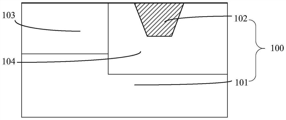
[0034] figure 1 It is a schematic cross-sectional structure diagram of a semiconductor structure.

[0035] Please refer to figure 1 , provide a substrate 100, the substrate includes a base 101, a field oxygen region 102 is formed in the substrate 100; a first photoresist layer is formed covering the surface of the field oxygen region 102 and part of the surface of the substrate 100 (not shown in the figure), implant N-type first dopant ions into the substrate 100 to form a body region 103, after forming the body region 103, remove the first photoresist layer; cover the body region 103 Forming a second photoresist layer (not shown in the figure), implanting P-type second dopant ions i...


PUM

PropertyMeasurementUnit
depthaaaaaaaaaa

Abstract

The invention discloses a semiconductor structure and a forming method thereof, and the method comprises the steps: providing a substrate which comprises a first region and a second region which are adjacent to each other; a gate layer is formed on the substrate, a part of the gate layer is located on the first region, and the other part of the gate layer is further located on the second region; forming a first well region in the first region; forming a second well region in the second region, wherein the conduction type of the second well region is different from that of the first well region; a part of the gate layer is used as a mask, first doping ions are doped in the first well region to form a first doping region, the conduction type of the first doping region is the same as that of the first well region, a dopant in the first doping region is diffused to the second region to form a transverse diffusion gradient, and the first doping region and the second region form a second doping region; meanwhile, the potential barrier height of the source end is increased, the potential barrier lowering effect is effectively restrained, the threshold voltage of the device is improved, and meanwhile the performance such as the breakdown voltage of the device is improved.

Description

technical field [0001] The invention relates to the field of semiconductor manufacturing, in particular to a semiconductor structure and a forming method thereof. Background technique [0002] LDMOS devices (Lateral Double-Diffused Metal Oxide Semiconductor Field Effect Transistor, Lateral Double-Diffused Metal Oxide Semiconductor Field Effect Transistor) in high-voltage power devices have good process compatibility with CMOS devices due to the characteristics of current flowing laterally on the device surface. At the same time, compared with traditional power devices, LDMOS devices are widely used because of their good characteristics of high breakdown voltage and low on-resistance. [0003] The contradiction between withstand voltage and on-resistance in conventional LDMOS devices is prominent. Nowadays, relevant researchers have proposed a variety of solutions, including surface variable doping technology, light doping technology, field plate, etc. In addition to the abo...

Claims


Application Information

Patent Timeline
Patent Type & Authority Applications(China)
IPC IPC(8): H01L29/78H01L29/06H01L21/336
Inventor 赵猛
Owner SEMICON MFG INT (SHANGHAI) CORP
Why Eureka
Try Eureka