Waveguide amplifier

A waveguide amplifier, silicon dioxide technology, used in lasers, laser devices, phonon exciters, etc., can solve the problem of immature erbium-doped waveguide technology

Pending Publication Date: 2022-04-08
AALTO UNIV FOUND
View PDF2 Cites 2 Cited by
  • Summary
  • Abstract
  • Description
  • Claims
  • Application Information

AI Technical Summary

Problems solved by technology

However, Erbium-doped waveguide technology is still immature when it comes to producing competitive building blocks for the silicon photonics industry

Method used


Image

  • Waveguide amplifier
  • Waveguide amplifier
  • Waveguide amplifier

Examples


example 1

[0072] In this example, a silicon nitride strip waveguide combined with a single Er:Al 2 o 3 Gain layer waveguide amplifier. First, optical-quality silicon dioxide was deposited on the silicon substrate of the device by low-pressure chemical vapor deposition, where the silicon dioxide layer was 1.4 μm thick. Next, a silicon nitride layer with a thickness of 600 nm was deposited on the silicon dioxide layer by plasma enhanced chemical vapor deposition.

[0073]The deposition of the silicon dioxide and silicon nitride layers was followed by deep UV lithography (248nm) and reactive ion etching.

[0074] Erbium oxide (Er 2 o 3 ) and alumina (Al 2 o 3 ) sequentially deposited on the surface of the waveguide channel to use about 150nm thick erbium-alumina (Er:Al 2 o 3 ) layer coating to form the waveguide channel and the whole device. By using Er(thd) 3 Erbium oxide was grown using trimethylaluminum (TMA) and water precursors, while aluminum oxide was grown using trimethyl...

example 2

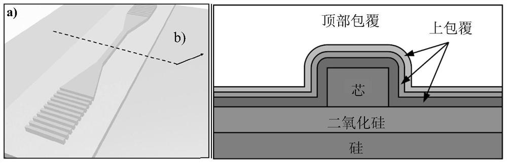
[0087] In this example, an Er:Al 2 o 3 Gain Layer Combination Multilayer Waveguide Amplifier Design. figure 1 b shows a cross-section of the device. Fabricated five different Er:Al on silicon substrates 2 o 3 Gain layers, and their spectral properties were investigated by photoluminescence (PL) characterization. Through numerical simulations, these layers are used to design waveguide amplifiers with improved gain characteristics.

[0088] characterize

[0089] Table 3 shows the cycle sequence and resulting film composition of the erbium-alumina active layer prepared in Example 2.

[0090] Table 3: Characteristics and preparation conditions of the Erbium-Al2O3 active layer deposited by atomic layer deposition

[0091]

[0092] The gain layer was then post-treated at 800° C. for 20 minutes.


PUM

PropertyMeasurementUnit
thicknessaaaaaaaaaa
thicknessaaaaaaaaaa
thicknessaaaaaaaaaa

Abstract

The invention relates to a waveguide amplifier and a waveguide amplifier device comprising the same. The invention also relates to a method for producing such a waveguide amplifier. The invention particularly relates to an erbium-doped waveguide amplifier with controlled doping concentration.

Description

technical field [0001] The present invention relates to a waveguide amplifier, a waveguide amplifier device including the waveguide amplifier, and a method of producing the waveguide amplifier. The invention relates in particular to waveguide amplifiers doped with rare earth materials, especially erbium. Background technique [0002] Modern information society is based on physical infrastructure where electronic devices play an important role. In addition to low-loss fiber optic transmission channels, information processing takes place via electronic routing and switching elements. Especially data centers have a lot of electronic equipment and circuit boards. The development of optical interconnects in the form of receivers is accelerating, especially in response to the ever-increasing information bit rates and high power consumption in data centers. The reason for this is simple: the lower the power consumption, the lower the cost per bit. For this to happen, reliable l...

Claims


Application Information

Patent Timeline
Patent Type & Authority Applications(China)
IPC IPC(8): H01S3/06H01S3/16H01S3/063H01S3/23
CPCH01S3/0637H01S3/0635H01S3/1608H01S3/1693H01S3/2308H01S3/0625H01S3/1636
Inventor 孙志培约翰·罗恩
Owner AALTO UNIV FOUND
Why Eureka
Try Eureka