Optical fiber panel cathode light window and preparation method thereof
An optical fiber panel and photocathode technology, which is applied in the field of glass surface treatment, can solve the problems of inability to meet the requirements of cathode sensitivity, difficult to achieve interface reflection, and narrow selection of photocathode substrate materials, so as to improve the photoelectron conversion efficiency and reduce the photon flux. Quantity loss, the effect of reducing the impact
- Summary
- Abstract
- Description
- Claims
- Application Information
AI Technical Summary
Problems solved by technology
Method used
Image
Examples
Embodiment 1
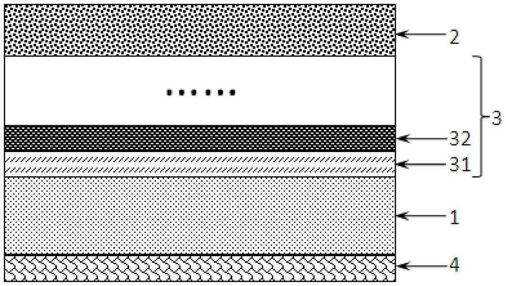
[0067] The optical fiber panel used in this embodiment is an array of light transmission and image transmission formed by regular arrangement of tens of millions, or even hundreds of millions of unit optical fibers, which are then melted and pressed. The fiber optic panel used in this embodiment has an outer diameter of 31 mm, a thickness of 5.6 mm, and both ends are flat. One side surface of the photocathode), the cross-section of the unit optical fiber is circular, and its silk diameter is 6 microns, and the cross-sectional ratio of the core layer and the cortex is 65 / 35. The cross-sectional ratio of the filament is 1.3%, the refractive index of the fiber core glass is 1.81, and the refractive index of the fiber skin glass is 1.51.
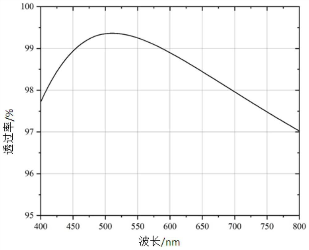
[0068] The outer surface of the fiber optic panel is coated with a second functional layer (double-layer anti-reflection coating), and the film adjacent to the fiber optic panel is Al 2 o 3 film, the other film away from the fiber optic panel ...
Embodiment 2
[0076] The fiber optic panel is the same as in Embodiment 1.
[0077] The micro-nano pits are formed by chemical etching, the etching solution is nitric acid solution, the pH value is preferably 3, the treatment time is 3 hours, and the treatment temperature is 50°C.
[0078] The second functional layer is the same as in Embodiment 1.
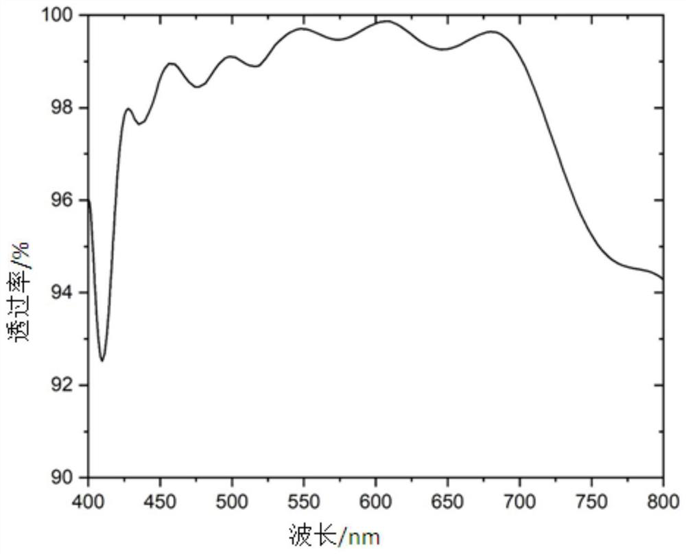
[0079] The first functional layer is a titanium dioxide layer, and the ion barrier layer is an aluminum oxide layer; the order of plating, the refractive index of the film layer, and the thickness of the film are shown in Table 2 below. The preparation method of the first functional layer and the ion barrier layer is atomic layer deposition technology.
[0080] Table 2
[0081] Layer order Membrane Refractive index nD Film thickness (nm) second functional layer -2 MgF 2
1.3849 83 second functional layer -1 Al 2 o 3
1.7643 30 Fiber optic panel 0 ---- ---- ---- ion barrier 1 al 2 ...
Embodiment 3
[0085] The fiber optic faceplate is the same as in Embodiment 1.
[0086] The micro-nano pits are formed by chemical etching. The corrosion solution is alkali solution, and KOH solution can be selected. The pH value is preferably 12.5. The processing time can be set according to the depth of the prepared pits. The processing temperature is 55°C and the processing time is 3 hours. .
[0087] The second functional layer is the same as in Embodiment 1.
[0088] The first functional layer is a titanium dioxide layer, and the ion barrier layer is an aluminum oxide layer; the order of plating, the refractive index of the film layer, and the thickness of the film are shown in Table 3 below. The preparation method of the first functional layer and the ion barrier layer is atomic layer deposition technology.
[0089] table 3
[0090] Layer order Membrane Refractive index nD Film thickness (nm) second functional layer -2 MgF 2
1.3849 83 second fun...
PUM
| Property | Measurement | Unit |
|---|---|---|
| thickness | aaaaa | aaaaa |
| thickness | aaaaa | aaaaa |
| surface roughness | aaaaa | aaaaa |
Abstract
Description
Claims
Application Information


