Power switch based on GaAs pHEMT technology and GaN technology
A power switch and process technology, applied in electronic switches, electrical components, pulse technology, etc., can solve the problems of difficult optimal design of converter parameters, high electromagnetic radiation and noise, and increased switching loss, etc., to achieve excellent power performance and low switching Effect of Loss, Operating Frequency and Gain Increase
- Summary
- Abstract
- Description
- Claims
- Application Information
AI Technical Summary
Problems solved by technology
Method used
Image

Examples
Embodiment 1
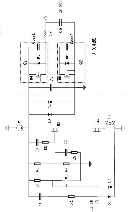
[0048] This embodiment proposes a power switch based on GaAs pHEMT process and GaN process, such as figure 1 As shown, including drive amplifier unit and switch circuit unit;
[0049] The input end of the drive amplifier unit receives a radio frequency input signal, and the output end is connected to the switch circuit unit; the output end of the switch circuit unit outputs a radio frequency output signal;
[0050] The drive amplifier unit includes transistors made based on GaAs pHEMT technology; the switch circuit unit includes transistors made based on GaN technology.
[0051] In order to better realize the present invention, further, the switch circuit unit includes a boost switch Q1, a boost switch Q2, a power inductor L2, an input capacitor C4, and an output capacitor C5;
[0052] The input capacitor C4 is connected to the ground after being connected to the DC voltage source V1;
[0053] The boost switch Q1 is connected between the DC voltage source V1 and the input en...
Embodiment 2
[0060] This embodiment is based on the above-mentioned embodiment 1, in order to better realize the present invention, further, as figure 1 As shown, the drive amplifier unit includes a first capacitor C1, a second capacitor C2, a third capacitor C3, a first resistor R1, a second resistor R2, a third resistor R3, a fourth resistor R4, a fifth resistor R5, a Six resistors R6, first transistor M1, second transistor M2, third transistor M3, first diode D1, second diode D2, third diode D3, fourth diode D4, DC voltage source V1, the first inductor L1;
[0061] One end of the first capacitor is connected to the anode of the DC voltage source V1, the other end is connected to the first resistor R1 and connected to the anode of the first diode D1 through the first resistor R1; the cathode of the first diode D1 connected to the ground;
[0062] One end of the second resistor R2 is connected to the anode of the DC voltage source V1, the other end is connected to the source of the firs...
Embodiment 3
[0084]In this embodiment, on the basis of the above-mentioned embodiment 2, in order to better realize the present invention, further, the gate widths of the first transistor M1 and the second transistor M2 are respectively 8×100 μm and 8×120 μm.
[0085] Further, the parameter of the power inductor L2 is 36nH.
[0086] Further, the value of the switch output capacitor Coss1 is 600 pF.
[0087] Further, the value of the switch output capacitor Coss2 is 600 pF.
[0088] Other parts of this embodiment are the same as those of Embodiment 2 above, so details are not repeated here.
PUM
| Property | Measurement | Unit |
|---|---|---|
| width | aaaaa | aaaaa |
Abstract
Description
Claims
Application Information