Method for etching magnetic tunnel junction of MRAM (Magnetic Random Access Memory)

A technology of magnetic tunnel junction and etching amount, which is applied in the fields of magnetic field-controlled resistors, electromagnetic device manufacturing/processing, semiconductor devices, etc., which can solve problems such as difficulty in meeting etching requirements, achieve improved etching effects, and improve TMR and service life, the effect of eliminating bottom deposits

Pending Publication Date: 2022-05-24
JIANGSU LEUVEN INSTR CO LTD
View PDF0 Cites 0 Cited by
  • Summary
  • Abstract
  • Description
  • Claims
  • Application Information

AI Technical Summary

Problems solved by technology

However, for smaller and denser MTJ junctions, it is more difficult to meet the above three etching requirements by conventional IBE etching or RIE etching

Method used


Image

  • Method for etching magnetic tunnel junction of MRAM (Magnetic Random Access Memory)
  • Method for etching magnetic tunnel junction of MRAM (Magnetic Random Access Memory)
  • Method for etching magnetic tunnel junction of MRAM (Magnetic Random Access Memory)

Examples


Embodiment 1

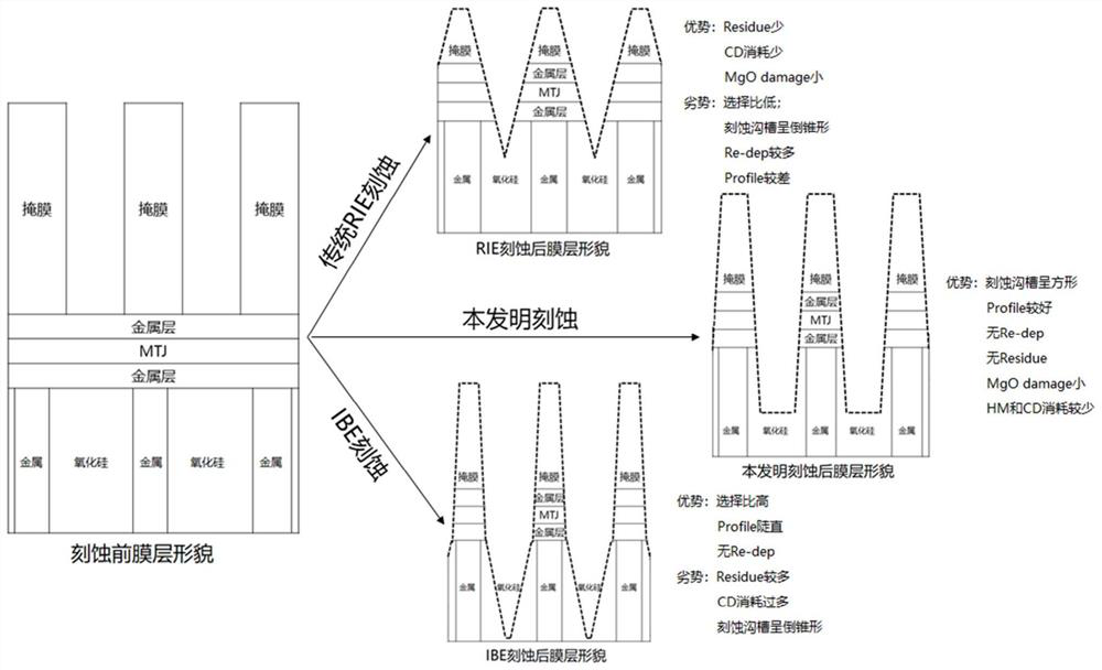
[0075] Step 1, the main engraving step is carried out using reactive ion etching: will be as follows Figure 2 The magnetic tunnel junction sample shown is passed into the RIE chamber for main engraving, and the main stepping energy is 500W source power, bias power is 600W, cavity pressure is 20mTorr, and etch gas is Kr.

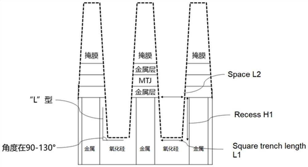
[0076] Reaction ion etching stops at the remaining 10nm of the lowest metal layer to a depth of 40nm of the bottom medium layer, in the present embodiment, a etching is preferably stopped at the remaining 5nm of the lowest metal layer, the etching amount is preferably t1 is preferably 35nm.

[0077] Step 2, the cleaning step is performed using a combination of reactive ion etching RIE + ion beam etching IBE

[0078] Step 21, reactive ion etching RIE: Through the vacuum chamber, the magnetic tunnel completed by the main engraving step of step 1 is knotted into a sample, and the secondary reaction ion etching is carried out. The parameters of the secondary reaction i...

Embodiment 2

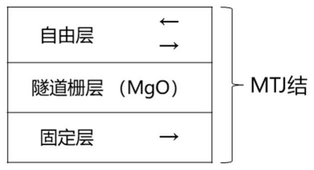
[0083] Step 1, the main engraving step is carried out using reactive ion etching: will be as follows Figure 4The magnetic tunnel junction sample shown is fed into the reaction ion chamber, the reaction ion etching ion source power is 600W, the bias voltage is 600V, the cavity pressure is 10mT, and the argon flow rate is 150 sccm. Among them, the magnetic tunnel junction sample to be etched includes the mask layer, cap layer, MTJ junction, bottom electrode layer and bottom medium layer from top to bottom. Reactive ion etching stops at 3 nm consumed at the bottom electrode layer. At this time, the amount of reaction ion etching is 20 nm.

[0084] Step 2, the use of reactive ion etching for cleaning step: the secondary etching process conditions are preferably: reactive ion pulse Pulse selection 5%, reaction ion source power Source 300W, bias voltage at 600V, cavity pressure 1.5mT, argon flow rate of 200sccm, etching 30nm to the seed layer, that is, the reaction ion etching amount t2...

Embodiment 3

[0089] Step 1, the main step is carried out by using ion beam etching: the magnetic tunnel junction sample is passed into the ion beam etching chamber, and the direction angle of the ion beam is selected as 25°, the energy is 600V, and the shielding gas is selected as argon gas etching. Among them, the magnetic tunnel junction sample includes the mask layer, cap layer, MTJ junction, bottom electrode metal layer and bottom medium layer from top to bottom. The bottom medium layer is nested at a medium distance with an electrode under metal equal to the number of masks in the mask layer, and the electrode under metal corresponds to the position of the mask. The ion beam etching stops at the remaining 5 nm of the lowest metal layer, that is, the ion beam etching amount t1 is 35 nm.

[0090] Step 2, the cleaning step is carried out by reactive ion etching: through the vacuum chamber, the magnetic tunnel junction sample from step 1 to complete the ion beam etching chamber is transferred ...


PUM

PropertyMeasurementUnit
thicknessaaaaaaaaaa

Abstract

The invention discloses an etching method of an MRAM (Magnetic Random Access Memory) magnetic tunnel junction, which comprises the following steps: step 1, carrying out a main etching step with the etching amount of t1 by adopting ion beam etching and/or reactive ion etching, wherein the direction angle of the ion beam is 10-60 degrees, and the bias voltage of the reactive ion etching is 400-1000V; the bias voltage of reactive ion etching is 50-400 V, the pulse duty ratio is 5%-50%, the ratio of t1 to t2 is larger than or equal to 0.5, and after the cleaning step is completed, the etching morphology on the bottom electrode or the bottom dielectric layer is a square groove; and step 3, in-situ protection: carrying out in-situ protection on the plated film. According to the method, RIE etching and IBE etching are combined, the etching effect on small-size dense magnetic tunnel junctions is remarkably improved through arrangement of the etching sequence and selection of etching parameters, and meanwhile the method can be suitable for etching of non-dense magnetic tunnel junctions. Therefore, the problems of low selection ratio and low steepness during dense pattern etching are solved. Furthermore, the TMR of the MTJ junction can be greatly improved, the service life of the MTJ junction can be greatly prolonged, and bottom deposition can be eliminated.

Description

Technical field [0001] The present invention relates to the field of magnetic random access memory, in particular an etching method of MRAM magnetic tunnel junction. Background [0002] At present, the widely used memory types are mainly SRAM (Static Random Access Memory), DRAM (Dynamic Random Access Memory) and Flash (Flash Memory). SRAM does not need to refresh the circuit to save the data stored internally, with high performance but low integration. DRAM is highly integrated and consumes low power, but requires circuit refresh to continuously save data. MrAM (Magnetic Random Access Memory) has the high-speed read and write capabilities of SRAM, as well as the high integration of DRAM, which can be written indefinitely, which can be used for systems that need to store data quickly and a lot, and maintain data after power outage, and can be quickly restored. In terms of "non-volatile" features, only MRAM and FLASH currently have this function, while Flash lacks the function of "...

Claims


Application Information

Patent Timeline
Patent Type & Authority Applications(China)
IPC IPC(8): H01L43/12H01L43/08H01L27/22
CPCH10B61/00H10N50/01H10N50/10H01L21/3065H10N59/00
Inventor 李佳鹤杨宇新彭泰彦许开东
Owner JIANGSU LEUVEN INSTR CO LTD
Why Eureka
Try Eureka