Preparation method of large-size flexible gallium nitride single crystal film

A gallium nitride single crystal, large-scale technology, applied in the semiconductor field, can solve the problems of easy-to-crack GaN film, poor heat dissipation of GaN film, high dislocation density, etc., achieve good heat dissipation performance and ductility, not easy to crack, and reduce dislocations effect of density

Active Publication Date: 2022-06-03
WESTLAKE UNIV
View PDF2 Cites 1 Cited by
  • Summary
  • Abstract
  • Description
  • Claims
  • Application Information

AI Technical Summary

Problems solved by technology

[0004] The purpose of the present invention is to provide a method for preparing a large-scale flexible gallium nitride single crystal film, which solves the problems of poor heat dissipation, poor quality, high dislocation density, large internal stress, easy cracking and other problems in the existing GaN growth and preparation process. GaN film is not easy to transfer and other issues

Method used


Image

  • Preparation method of large-size flexible gallium nitride single crystal film
  • Preparation method of large-size flexible gallium nitride single crystal film
  • Preparation method of large-size flexible gallium nitride single crystal film

Examples


Embodiment 1

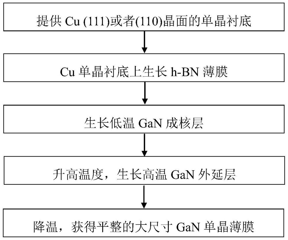
[0046] A preparation method of a large-scale flexible gallium nitride single crystal film, comprising the following steps:

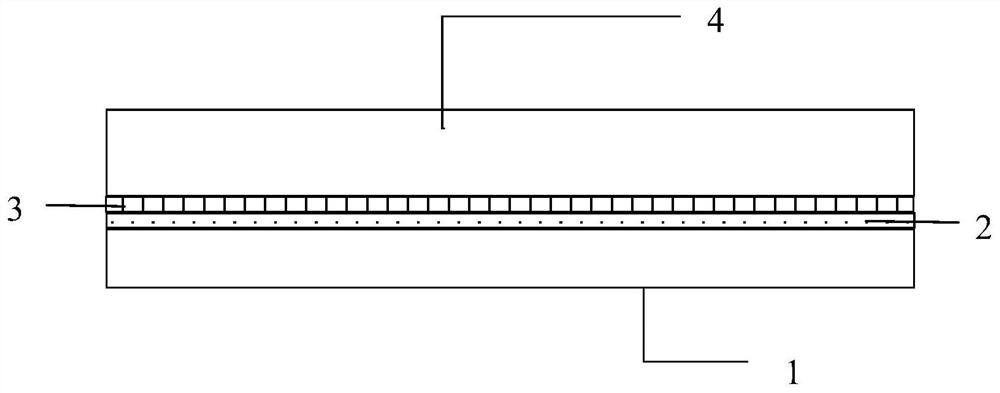
[0047] Step 1: Provide Cu single crystal substrate 1

[0048] The crystal plane of Cu single crystal substrate 1 is (111), and the thickness is 150 μm.

[0049] Step 2: Grow the h-BN thin film layer 2 on the Cu single crystal substrate 1 of Step 1

[0050] The chemical vapor deposition (CVD) method was used, borane ammonia was used as the precursor, the purity of the borane ammonia was 97%, the growth pressure was 160Pa, the precursor temperature was set to 75°C, and the growth temperature on the Cu single crystal substrate 1 was The temperature was 1040 °C, the growth time was 1 h, and the growth thickness was 200 nm.

[0051] Step 3: grow a low temperature GaN nucleation layer 3 on the h-BN thin film layer 2 grown in step 2

[0052] Using the HVPE process, the temperature is set to 680°C, the pressure is set to 700 Torr, the V / III is set to 130, the...

Embodiment 2

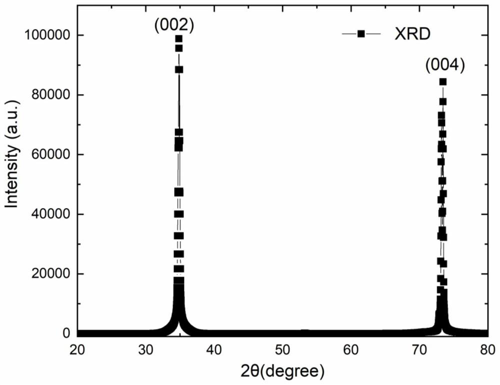
[0064] The difference between this embodiment and Embodiment 1 is that the crystal plane of the Cu single crystal substrate 1 is (110), and the dislocation density test of SEM, AFM and cathode fluorescence is also carried out on it, and the obtained results are the same as those of Embodiment 1. quite.

Embodiment 3

[0066] The difference between this embodiment and Embodiment 1 is that the crystal plane of the Cu single crystal substrate 1 is (100), and the resulting GaN film has poor uniformity and large roughness. The SEM inspection results are as follows Figure 8 shown.


PUM

PropertyMeasurementUnit
thicknessaaaaaaaaaa
thicknessaaaaaaaaaa
thicknessaaaaaaaaaa

Abstract

The invention discloses a preparation method of a large-size flexible gallium nitride single crystal thin film, and solves the problems that a GaN thin film is poor in heat dissipation, poor in quality, high in dislocation density, large in internal stress, easy to crack, not easy to transfer and the like in the existing GaN growth and preparation process. The method comprises the following steps: step 1, providing a Cu single crystal substrate; step 2, growing an h-BN thin film layer on the Cu single crystal substrate in the step 1; step 3, growing a low-temperature GaN nucleating layer on the h-BN thin film layer grown in the step 2; 4, continuously and epitaxially growing a GaN epitaxial layer on the low-temperature GaN nucleating layer grown in the step 3; and step 5, cooling the high-temperature GaN epitaxial layer obtained in the step 4 to room temperature to obtain a flat GaN single crystal film. The method has the advantages that the generated GaN single crystal film is good in heat dissipation, good in quality, low in dislocation density, low in roughness, easy to strip and the like.

Description

technical field [0001] The invention relates to the technical field of semiconductors, in particular to a preparation method of a large-size flexible gallium nitride single crystal thin film. Background technique [0002] Gallium Nitride (GaN) has a band gap of 3.4eV. Due to its high carrier mobility, fast carrier radiative recombination, and long-term stability and reliability, it is a promising candidate for high-frequency and high-power applications. And wide bandgap semiconductor materials for photoelectric conversion scenarios can be made into metal semiconductor field effect transistors (MESFETs), high electron mobility transistors (HEMTs), LEDs and photodetectors (PDs), etc. [0003] Regarding the growth of GaN thin films, there are generally three growth methods: molecular beam epitaxy (MBE), metal organic chemical vapor deposition (MOCVD), and hydride vapor phase epitaxy (HVPE). At present, the more common method is to epitaxially prepare the MOCVD method on a hete...

Claims


Application Information

Patent Timeline
Patent Type & Authority Applications(China)
IPC IPC(8): C30B29/40C30B23/02C30B25/18
CPCC30B29/406C30B25/183C30B23/025Y02P70/50
Inventor 杨军孔玮马亚庆
Owner WESTLAKE UNIV
Why Eureka
Try Eureka