

Method for preparing vertical cavity laser by transferring perovskite thin film
A technology of thin film transfer and perovskite, which is applied in the field of lasers, can solve the problems of unfavorable optical properties of laser devices, etc., and achieve the effects of easy industrial mass production, high flatness, and large transfer film area
- Summary
- Abstract
- Description
- Claims
- Application Information
AI Technical Summary
Problems solved by technology
Method used
Image

Examples
preparation example Construction
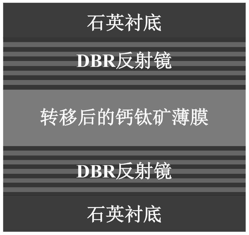
[0052] In the present invention, the preparation method of the first DBR mirror substrate spin-coated with the first perovskite polycrystalline thin film preferably includes the following steps:
[0053] Prepare a first DBR mirror layer on the surface of the substrate base;
[0054] A first perovskite polycrystalline film is spin-coated on the surface of the first DBR mirror layer, and after annealing treatment, a first DBR mirror substrate spin-coated with the first perovskite polycrystalline film is obtained.
[0055] In the present invention, the substrate base is preferably a quartz substrate, a silicon substrate, a sapphire substrate or a mica substrate. The present invention has no special requirements on the method of preparing the first DBR mirror layer, and the method can be prepared by a method well known to those skilled in the art.
[0056] In the present invention, the spin coating includes low-speed spin-coating and high-speed spin-coating performed in sequence,...
Embodiment 1
[0076] A vertical cavity laser based on a quasi-2D perovskite polycrystalline thin film was fabricated by a large-area perovskite thin film transfer method through the following steps:
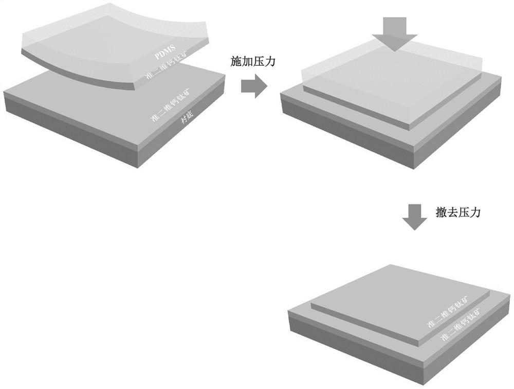
[0077] (1) Mix the base and the curing agent in a weight ratio of 10:1, and stir for 5 minutes to make them fully mixed. Then vacuum was applied for 30 min to completely remove air bubbles in the mixed solution. Then use atomically flat silicon as the substrate, pour the mixed solution, and vacuum again for 10 min. It was put into an oven at 80° C. for 1 h to be cured, thereby preparing a large-size PDMS (polydimethylsiloxane) flexible substrate.
[0078] (2) Put the prepared PDMS substrate into an ozone-plasma apparatus, work at a medium power of 15W for 3 minutes, and use the plasma to bombard the surface of the flexible substrate to increase the surface energy of the substrate, which can make the originally hydrophobic PDMS substrate. The surface is hydrophilic.
[0079] (3) Within 30 mi...
PUM
| Property | Measurement | Unit |
|---|---|---|
| thickness | aaaaa | aaaaa |
| area | aaaaa | aaaaa |
| thickness | aaaaa | aaaaa |
Abstract
Description
Claims
Application Information