Unlock instant, AI-driven research and patent intelligence for your innovation.

Silicon carbide single crystal substrate, preparation method and semiconductor device

A silicon carbide single crystal and semiconductor technology, which is applied in semiconductor/solid-state device manufacturing, chemical instruments and methods, crystal growth, etc., can solve the problems that the yield rate of semiconductor devices cannot be significantly improved, reduce the failure probability, improve the yield rate, Effect of Reducing Dislocation Density

Pending Publication Date: 2022-06-07
BEIJING TIANKE HEDA SEMICON CO LTD +2
View PDF0 Cites 0 Cited by
  • Summary
  • Abstract
  • Description
  • Claims
  • Application Information

AI Technical Summary

Problems solved by technology

At present, the dislocation density of semiconductor devices based on silicon carbide single crystals on the market is still high. In recent years, with the advancement of technology, the dislocation density has gradually decreased, but it still cannot significantly improve the yield of semiconductor devices.

Method used


Image

  • Silicon carbide single crystal substrate, preparation method and semiconductor device
  • Silicon carbide single crystal substrate, preparation method and semiconductor device
  • Silicon carbide single crystal substrate, preparation method and semiconductor device

Examples


preparation example Construction

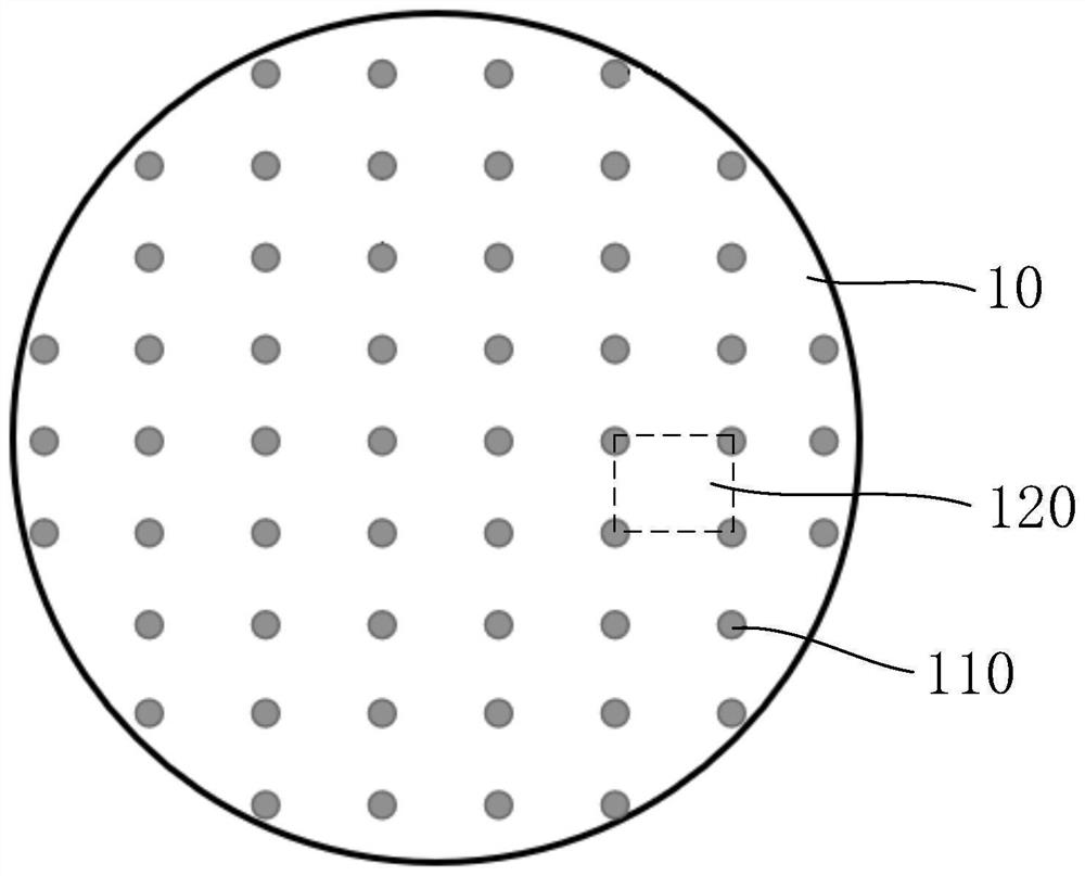
[0062] The present invention also provides a method for preparing a silicon carbide single crystal substrate, which is used to prepare the silicon carbide single crystal substrate provided in any of the above embodiments, see Figure 4 , the preparation method of the silicon carbide single crystal substrate comprises the following steps:

[0063] S01: patterning the pinning region on the seed crystal growth surface and annealing;

[0064] S02: use physical vapor transport method to grow silicon carbide single crystal;

[0065] S03: cutting the silicon carbide single crystal and grinding and polishing.

[0066] In step S01, the desired shape and distribution state of the pinning region 110 of the silicon carbide single crystal substrate are first determined, a pattern is made on the growth surface of the seed crystal according to the shape of the pinning region 110, and the processed seed crystal is processed. An annealing treatment is performed, and the annealing treatment i...


PUM


Abstract

The invention discloses a silicon carbide single crystal substrate, which comprises a first surface and a second surface, the first surface comprises pinning areas and a workpiece area, the pinning areas are manually arranged potential wells so as to concentrate the dislocation of the areas around the pinning areas on the pinning areas, and the first surface is provided with a plurality of pinning areas; the workpiece area is used for manufacturing a semiconductor device, and the pinning area is arranged around the workpiece area, so that the dislocation density of a central area of the workpiece area is smaller than that of an edge area. According to the silicon carbide single crystal substrate provided by the invention, the pinning region is arranged around the workpiece region to concentrate the dislocation on the workpiece region on the edge of the workpiece region, so that the dislocation density of the central region of the workpiece region is reduced, and the central region of the workpiece region is used for manufacturing an effective region of a semiconductor device, namely a region for applying voltage on the semiconductor device; the dislocation density of the effective area can be obviously reduced, the failure probability of the effective area is reduced, and the yield of the semiconductor device is improved.

Description

technical field [0001] The present invention relates to the technical field of silicon carbide single crystal manufacturing, in particular to a silicon carbide single crystal substrate, a preparation method and a semiconductor device. Background technique [0002] With the continuous innovation of semiconductor technology, silicon carbide (SiC) in the third-generation wide bandgap material has developed rapidly due to its excellent material properties and the huge application prospects presented by silicon carbide devices. The preparation of silicon carbide crystals and related devices The research has always been a frontier research hotspot at home and abroad. Silicon carbide single crystal has various superior properties such as large forbidden band width, high breakdown electric field, high thermal conductivity, fast electron saturation drift rate, high chemical stability, and strong radiation resistance. Preferred choice for radiation, high power semiconductor device ma...

Claims


Application Information

Patent Timeline
IPC IPC(8): H01L21/02H01L21/04C30B23/02C30B29/36C30B33/02B24B37/00B28D5/04
CPCH01L21/02008H01L21/02013H01L21/0445C30B29/36C30B33/02C30B23/02B28D5/045B24B37/00H01L29/045C30B23/025H01L29/1608H01L29/32
Inventor 娄艳芳刘春俊王光明姚静雍庆彭同华杨建
Owner BEIJING TIANKE HEDA SEMICON CO LTD
Features
  • R&D
  • Intellectual Property
  • Life Sciences
  • Materials
  • Tech Scout
  • Unparalleled Data Quality
  • Higher Quality Content
  • 60% Fewer Hallucinations
Learn More