Gradient machining system and method for atomic-scale surface and structure

A processing system and processing method technology, applied in metal processing equipment, manufacturing tools, welding equipment, etc., can solve the problems of unsuitable production, spontaneous etching of net deposition, low removal rate, etc., to avoid connection problems and repeated positioning. Difficulty, reduce lattice damage, and improve the effect of machining accuracy

Pending Publication Date: 2022-06-21
TIANJIN UNIV
View PDF8 Cites 1 Cited by
  • Summary
  • Abstract
  • Description
  • Claims
  • Application Information

AI Technical Summary

Problems solved by technology

[0003] Atomic layer etching (ALE) can remove atomic layers through self-limiting chemical reactions to achieve atomic-level surface roughness, but there are problems such as low removal rate, selectivity loss, net deposition and spontaneous etching.
Based on atomic force microscopy (AFM), scanning tunneling microscopy (STM) and scanning probe microscopy (SPM), single atoms can be manipulated for atomic-level structure preparation and doping, but the extremely low work efficiency is not yet suitable for production practice.

Method used


Image

  • Gradient machining system and method for atomic-scale surface and structure
  • Gradient machining system and method for atomic-scale surface and structure
  • Gradient machining system and method for atomic-scale surface and structure

Examples


Embodiment Construction

[0040] It should be noted that the embodiments in the present application and the features of the embodiments may be combined with each other in the case of no conflict. The present invention will be described in detail below with reference to the accompanying drawings and in conjunction with the embodiments.

[0041]It should be noted that, unless otherwise specified, all technical and scientific terms used in this application have the same meaning as commonly understood by one of ordinary skill in the art to which this application belongs.

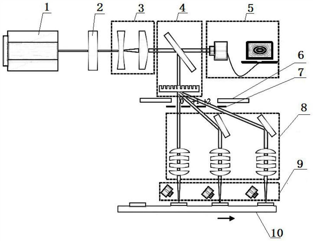
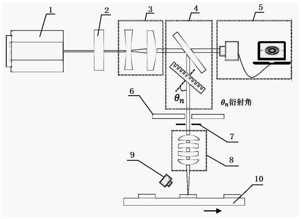
[0042] figure 1 , figure 2 The processing systems built according to the two processing methods of the present invention respectively include:

[0043] Light source 1, using an ultraviolet femtosecond laser.

[0044] The energy adjuster 2 is used to adjust the initial energy incident on the processing system to ensure that the energy incident on the surface of the grating meets the diffraction requirements of the grating and does not...


PUM


Abstract

The invention relates to an atomic-scale surface and structure gradient machining system and method, and the system is sequentially provided with an energy regulator, a light beam shaping module and a grating beam splitting module along a light path, and the grating beam splitting module is used for splitting a machining light beam into a light beam which is suitable for the machining of each precision grade and has required irradiation energy density; the diaphragm is used for limiting the diffracted light beams entering a subsequent processing system; the optical switch is used for controlling whether the processing light beam is emitted or not; and the light beam focusing module is used for focusing light beams. The machining method comprises the steps of fixing the grating and moving a workpiece for different-precision machining; or the workpiece is fixed, and the grating is adjusted to realize in-situ machining with different precisions. According to the invention, cross-scale micron-scale, nano-scale and atomic-scale material removal is realized, the integration degree of the processing system is high, and the problem of connection and difficulty in repeated positioning caused by various processing methods and equipment are avoided; and by means of the ionization effect of high photon energy and fine regulation and control of ultrashort pulses on the material, lattice damage to the final surface is effectively reduced, and the machining precision is improved.

Description

technical field [0001] The invention belongs to the field of precision, ultra-precision, atomic and near-atomic scale manufacturing, in particular to a gradient processing system and method for atomic-level surfaces and structures. Background technique [0002] With the rapid development of information technology and various fields, the manufacture of important core devices such as quantum chips, photonic chips and biochips has put forward higher and higher requirements for surface quality and processing accuracy, and even requires the realization of atomically flat surfaces and structures. Among the existing subtractive manufacturing technologies, ultra-precision diamond processing technology can achieve micro- and nano-scale machining accuracy, and ultra-precision grinding or polishing technology can achieve nano-scale or sub-nanometer surface roughness. Ion beam processing, electron beam processing and extreme ultraviolet (EUV) lithography can achieve nano-scale material ...

Claims


Application Information

Patent Timeline
Patent Type & Authority Applications(China)
IPC IPC(8): B23K26/36B23K26/0622B23K26/064B23K26/067
CPCB23K26/36B23K26/0624B23K26/064B23K26/0676
Inventor 房丰洲吴珊王金石
Owner TIANJIN UNIV
Why Eureka
Try Eureka