Preparation method of charge transport layer and light emitting diode

A charge transport layer, light-emitting diode technology, applied in circuits, electrical components, electro-solid devices, etc., can solve the problems of low exciton mobility and dissociation, and achieve high exciton mobility, high efficiency and stable performance. Effect

Pending Publication Date: 2022-06-28
TCL CORPORATION
View PDF0 Cites 0 Cited by
  • Summary
  • Abstract
  • Description
  • Claims
  • Application Information

AI Technical Summary

Problems solved by technology

[0006] An object of the present invention is to overcome the above-mentioned deficiencies in the prior art, and provide a preparation method of a charge transport layer and a light-emitting diode to solve the problem that the existing colloidal metal oxide nanocrystals form a charge transport layer with local defects and make the exciton mobility Technical issues with low or dissociation phenomena

Method used


Image

  • Preparation method of charge transport layer and light emitting diode
  • Preparation method of charge transport layer and light emitting diode
  • Preparation method of charge transport layer and light emitting diode

Examples


preparation example Construction

[0021] In one aspect, embodiments of the present invention provide a method for preparing a charge transport layer. The preparation method of the charge transport layer includes using a first solution containing a functional material to form a first film layer and using a second solution containing a charge transport material to form a second film layer, and making the first film layer and the second film layer The film layers are adjacent to each other, and then remove the functional material to obtain the charge transport layer; or use the mixed solution of the first solution and the second solution to form a mixed film layer, and then remove the functional material to obtain the charge transport layer. Therefore, in the embodiment, the preparation method of the charge transport layer includes at least the following three preparation methods of the charge transport layer:

[0022] The first preparation method of the charge transport layer:

[0023] The process flow of the f...

Embodiment 1

[0062] This embodiment provides a QLED light-emitting diode and a manufacturing method thereof.

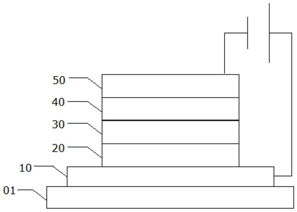
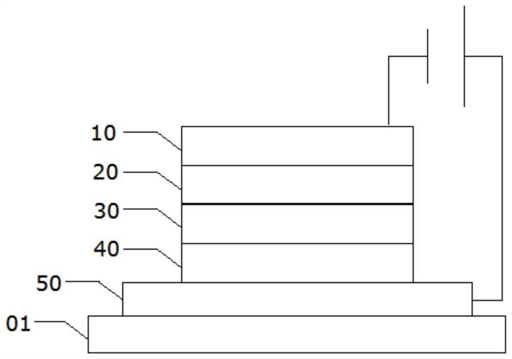
[0063] The structure of the QLED light-emitting diode is as follows figure 2 The positive quantum dot light-emitting diode shown has the structure of ITO / PEDOT:PSS(30nm)hole transport layer(30nm) / CdSe / ZnS(40nm) / electron transport layer(40nm) / Ag(120nm). Among them, " / " expresses the connection relationship of the layer structure of the layered bonding.

[0064] The preparation method of the QLED of the present embodiment includes the following steps:

[0065] S1: providing a substrate on which a bottom electrode (anode) is formed;

[0066] S2: sequentially depositing an organic hole injection layer, an organic hole transport layer, and a quantum dot light-emitting layer on the bottom electrode;

[0067] S3: First deposit a zinc oxide-ethanol solution on the surface of the quantum dot light-emitting layer to form a zinc oxide electron transport wet film layer, which is also the ...

Embodiment 2

[0070] This embodiment provides a QLED light-emitting diode and a manufacturing method thereof.

[0071] The structure of the QLED light-emitting diode is as follows figure 2 The positive quantum dot light-emitting diode shown has the same structure as that of Example 1.

[0072] The preparation method of the QLED of the present embodiment includes the following steps:

[0073] S1: providing a substrate on which a bottom electrode (anode) is formed;

[0074] S2: sequentially depositing an organic hole injection layer, an organic hole transport layer, and a quantum dot light-emitting layer on the bottom electrode;

[0075] S3: deposit triethylamine-acetone solution on the surface of the quantum dot light-emitting layer first to form a first film layer of triethylamine; then deposit zinc oxide-ethanol solution on the surface of the first film layer to form a zinc oxide electron transport wet film layer to form a zinc oxide-triethylamine composite wet film layer, and then hea...


PUM


Abstract

The invention discloses a preparation method of a charge transport layer and a light-emitting diode. The preparation method of the charge transport layer comprises the following steps: forming a first film layer by using a first solution containing a functional material, forming a second film layer by using a second solution containing a charge transport material, and enabling the first film layer and the second film layer to be in contact with each other, or forming a mixed film layer by using a mixed solution of the first solution and the second solution; removing the functional material to obtain the charge transport layer; the functional material is an organic matter containing an electron-donating group, the surface of the charge transport material is provided with a metal cation dangling bond, and the electron-donating group can be combined with the metal cation dangling bond. The light-emitting diode comprises an electron transport layer and/or a hole transport layer, and the electron transport layer and/or the hole transport layer are/is prepared and formed according to the preparation method of the charge transport layer.

Description

technical field [0001] The invention belongs to the field of optoelectronic technology, and in particular relates to a preparation method of a charge transport layer and a light emitting diode. Background technique [0002] Charge transport layers (CTLs), namely electron transport layers (ETL) and hole transport layers (HTL), are essential components for state-of-the-art solution-processed optoelectronic devices. CTL affects not only charge injection within the active layer, but also many other fundamental physical processes of device operation, such as interfacial charge recombination and light extraction (or light absorption) in LEDs (or solar cells). [0003] In recent years, colloidal metal oxide nanocrystals have attracted great interest as CTLs. The best example is ETL based on colloidal ZnO nanocrystals, which has been used in several of the best performing prototype devices. Furthermore, colloidal oxide nanocrystals are fully compatible with large-scale industrial ...

Claims


Application Information

Patent Timeline
Patent Type & Authority Applications(China)
IPC IPC(8): H01L51/56H01L51/50
CPCH10K71/15H10K71/811H10K71/40H10K50/15H10K50/16H10K71/00H10K85/631H10K71/12H10K50/115Y02E10/549H10K85/00H10K2102/00
Inventor 陈开敏
Owner TCL CORPORATION
Why Eureka
Try Eureka