Frequency chip entangled two-photon source

A frequency slice and two-photon technology, which is applied in the field of quantum information science, can solve the problems of low efficiency of entangled photon pairs, low entanglement purity of frequency slices, and low generation rate of entangled photon pairs, so as to achieve miniaturization, integration, and high practicality. Sexual, high-brightness effect

Active Publication Date: 2022-07-15
UNIV OF ELECTRONICS SCI & TECH OF CHINA
View PDF23 Cites 0 Cited by
  • Summary
  • Abstract
  • Description
  • Claims
  • Application Information

AI Technical Summary

Problems solved by technology

[0004] The current method of generating frequency sheet entangled photon pairs through bulk second-order nonlinear crystals usually needs to be realized through a spatial optical path, which cannot meet the needs of system miniaturization and integration; and the third-order nonlinearity through spontaneous four-wave mixing process The process produces entangled photon pairs relatively inefficiently, resulting in a low rate of entangled photon pairs
At the same time, in the scheme of using the spontaneous four-wave mixing effect to generate frequency plate entangled photon pairs, the method of injecting energy-time entangled photon pairs into the non-equilibrium Mach-Zehnder interferometer is a main technical route. The pure output of this method is The associated photon pairs are in a mixed state, the purity of the frequency sheet entanglement is low, and time domain filtering is required in the application process

Method used


Image

  • Frequency chip entangled two-photon source
  • Frequency chip entangled two-photon source
  • Frequency chip entangled two-photon source

Examples


Embodiment Construction

[0030] The principles and features of the present invention will be described below with reference to the accompanying drawings. The examples are only used to explain the present invention, but not to limit the scope of the present invention.

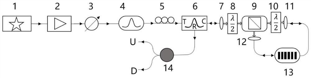
[0031] like figure 1 As shown, a frequency slice entangled two-photon source provided by the first embodiment of the present invention includes a pump laser source 1, an optical amplifier 2, a tunable optical attenuator 3, an optical filter 4, and a polarization controller 5 connected in sequence And the dense wavelength division multiplexer 6, wherein, the polarization controller 5 is connected with the transmission end (T end) of the dense wavelength division multiplexer 6;

[0032] The frequency plate entangled two-photon source further includes a first half-wave plate 8, a second half-wave plate 10, a spatial light polarization beam splitter 9, a first fiber collimator 7, a second fiber collimator 11, a third a fiber collimator 12,...


PUM

PropertyMeasurementUnit
wavelengthaaaaaaaaaa

Abstract

The invention relates to a frequency-bin entangled two-photon source, and belongs to the technical field of quantum information science. According to the frequency chip entangled two-photon source, on the basis of an improved Sagnac ring structure, correlated photon pairs are generated through a second harmonic generation process and a spontaneous parametric down-conversion process which are cascaded in a cross-polarization laser bidirectional pumping optical fiber coupling second-order nonlinear crystal waveguide; and frequency chip entangled photon pairs are generated through polarization control, quantum interference and polarization beam splitting. Two photons obtained through the structure have the advantages of being high in brightness and purity, miniaturization and integration of the frequency chip entangled two-photon source structure can be achieved, existing mature optical fiber communication devices can be adopted as the devices used in the frequency chip entangled two-photon source structure, and high practicability is achieved.

Description

technical field [0001] The invention belongs to the field of quantum information science and technology, and particularly relates to a frequency slice entangled two-photon source. Background technique [0002] Frequency slice entangled photon pairs are an important resource in quantum information technology and have potential applications in quantum precision measurement, quantum cryptography, quantum communication in noisy channels, and delocalized dispersion cancellation in quantum interferometers. . [0003] The generation of frequency-plate entangled photon pairs usually requires nonlinear optical processes in nonlinear optical media, and common processes include second-order nonlinear optical processes and third-order nonlinear optical processes. For example, the spontaneous parametric down-conversion process in nonlinear crystals such as periodically polarized lithium niobate crystal (PPLN) and periodically polarized potassium titanate phosphate crystal (PPKTP), and t...

Claims


Application Information

Patent Timeline
Patent Type & Authority Applications(China)
IPC IPC(8): G02F1/377G02F1/355G02F1/35G02B27/28
CPCG02F1/377G02F1/3551G02F1/353G02F1/3501G02B27/283
Inventor 周强李加睿袁晨智范云茹邓光伟宋海智王浟
Owner UNIV OF ELECTRONICS SCI & TECH OF CHINA
Why Eureka
Try Eureka