Multi-layer alloy diffusion barrier layer for Cu interconnection integrated circuit and preparation method of multi-layer alloy diffusion barrier layer

A technology for integrated circuits and barrier layers, which is applied in the field of multilayer alloy diffusion barrier layers for Cu interconnected integrated circuits and its preparation, can solve the problems of Cu atom diffusion, etc., and achieve increased diffusion probability, increased activation energy, and low resistivity Effect

Active Publication Date: 2022-07-22
亚芯半导体材料(江苏)有限公司 +1
View PDF7 Cites 1 Cited by
  • Summary
  • Abstract
  • Description
  • Claims
  • Application Information

AI Technical Summary

Problems solved by technology

[0006] The invention provides a multi-layer alloy diffusion barrier layer for Cu interconnected integrated circuits and its preparation method to solve the problem that Cu atoms are easy to diffuse along the grain boundaries of polycrystalline structures

Method used


Image

  • Multi-layer alloy diffusion barrier layer for Cu interconnection integrated circuit and preparation method of multi-layer alloy diffusion barrier layer

Examples


preparation example Construction

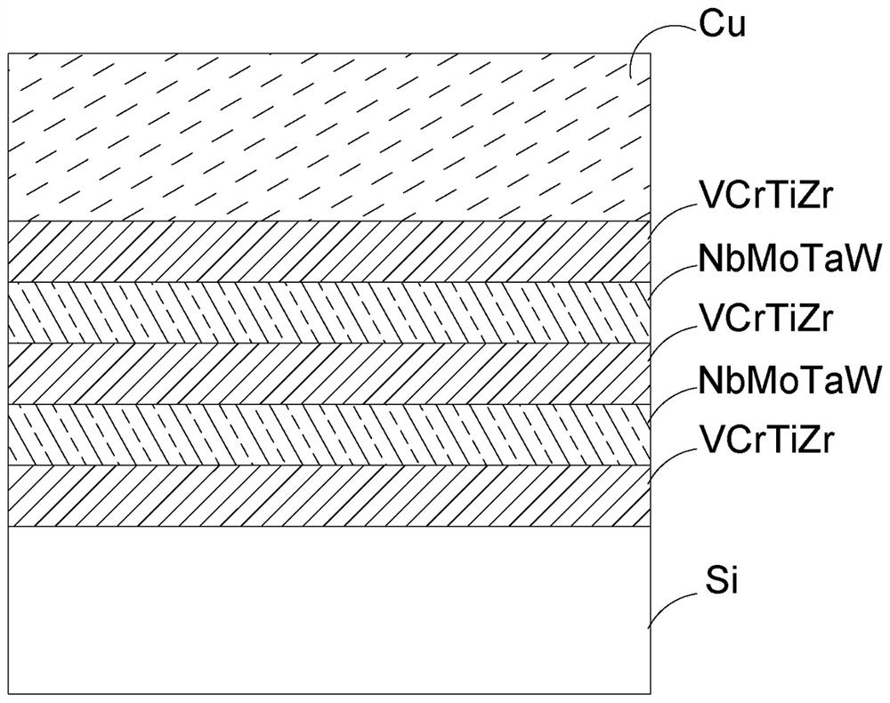
[0023] In another aspect, the present invention also provides a method for preparing a multi-layer alloy diffusion barrier layer for Cu interconnection integrated circuits, comprising the following steps: Step S1, vacuum smelting to obtain a NbMoTaW high-entropy alloy target and a VCrTiZr high-entropy alloy target In step S2, the single crystal Si substrate is cleaned by ultrasonic oscillation to obtain a Si substrate layer; in step S3, the NbMoTaW high-entropy alloy target and the VCrTiZr high-entropy alloy target are pre-sputtered and cleaned; in step S4, the VCrTiZr high-entropy alloy target is cleaned by pre-sputtering. The alloy target is sputtered on the Si substrate layer by a DC magnetron sputtering process to form a VCrTiZr high-entropy alloy coating; step S5, the NbMoTaW high-entropy alloy target is sputtered on the VCrTiZr high-entropy alloy coating by a DC magnetron sputtering process. layer to form a NbMoTaW high-entropy alloy coating; step S6, repeat steps S4 and ...

Embodiment 1

[0031] Mix Nb, Mo, Ta, and W in an equimolar ratio, and smelt 5 times in a vacuum electric furnace to obtain a NbMoTaW high-entropy alloy target with uniform composition; V, Cr, Ti, and Zr are mixed in an equimolar ratio, and smelted in a vacuum electric furnace 5 times to obtain a VCrTiZr high-entropy alloy target with uniform composition; before sputtering the high-entropy alloy intermediate coating, the Si substrate was ultrasonically cleaned with acetone, alcohol and deionized water in turn to remove surface oxides or impurities; The impurities on the VCrTiZr and NbMoTaW targets were cleaned by pre-sputtering, the power was 30 W, and the time was 2 minutes; the prepared VCrTiZr high-entropy alloy targets were sputtered on the Si lining by a DC magnetron sputtering process in an Ar atmosphere. On the bottom layer, a VCrTiZr high-entropy alloy coating is formed, when the base pressure reaches 2.0×10 −4 At Pa, argon gas was introduced, the flow rate was 25sccm, the working pr...

Embodiment 2

[0035] Mix Nb, Mo, Ta, and W in an equimolar ratio, and smelt 5 times in a vacuum electric furnace to obtain a NbMoTaW high-entropy alloy target with uniform composition; V, Cr, Ti, and Zr are mixed in an equimolar ratio, and smelted in a vacuum electric furnace 5 times to obtain a VCrTiZr high-entropy alloy target with uniform composition; before sputtering the high-entropy alloy intermediate coating, the Si substrate was ultrasonically cleaned with acetone, alcohol and deionized water in turn to remove surface oxides or impurities; The impurities on the VCrTiZr and NbMoTaW targets were cleaned by pre-sputtering, the power was 30 W, and the time was 2 minutes; the prepared VCrTiZr high-entropy alloy targets were sputtered on the Si lining by a DC magnetron sputtering process in an Ar atmosphere. On the bottom layer, a VCrTiZr high-entropy alloy coating is formed, when the base pressure reaches 2.0×10 −4 At Pa, argon gas was introduced, the flow rate was 25sccm, the working pr...


PUM

PropertyMeasurementUnit
thicknessaaaaaaaaaa
thicknessaaaaaaaaaa
purityaaaaaaaaaa

Abstract

The invention belongs to the technical field of semiconductor integrated circuits, and particularly relates to a multi-layer alloy diffusion barrier layer for a Cu interconnection integrated circuit and a preparation method thereof, and the multi-layer alloy diffusion barrier layer sequentially comprises a Si substrate layer, a high-entropy alloy middle barrier layer and a Cu film from bottom to top; the high-entropy alloy middle barrier layer sequentially comprises a first coating, a second coating, a third coating, a fourth coating and a fifth coating from top to bottom; according to the preparation method, NbMoTaW and VCrTiZr high-entropy alloy is used as a target material, a direct-current magnetron sputtering method is adopted, and a coating is sputtered on a Si base body layer to obtain the high-entropy alloy diffusion impervious layer of a Si-VCrTiZr-NbMoTaW-VCrTiZr-NbMoTaW-VCrTiZr-Cu composite structure. The obtained Cu interconnection integrated circuit high-entropy alloy diffusion impervious layer can still keep excellent thermal stability and diffusion impervious performance after being annealed at the high temperature of 400-750 DEG C for 30 min, and has wide application prospects in Cu interconnection integrated circuits.

Description

technical field [0001] The invention belongs to the technical field of semiconductor integrated circuits, and in particular relates to a multi-layer alloy diffusion barrier layer for Cu interconnection integrated circuits and a preparation method thereof. Background technique [0002] Since the development of integrated circuits (ICs) about 60 years ago, aluminum (Al) and silicon dioxide (SiO 2 ) has been widely used as a conductor and insulating material in the manufacture of microprocessors. Continuing reductions in feature size and the explosive increase in transistor counts in microprocessors have led to an increase in so-called gate delays as technology demands have grown. To solve this problem, new wiring materials with a lower resistivity than Al and a lower dielectric constant than conventional SiO must be used 2 dielectric material as an alternative. IBM announced in 1997 that it would replace aluminum with copper as an interconnect material in semiconductor proc...

Claims


Application Information

Patent Timeline
Patent Type & Authority Applications(China)
IPC IPC(8): H01L23/532H01L21/768C23C14/35C23C14/34C23C14/16C22C30/00C22C1/02
CPCH01L23/53238H01L21/7685H01L21/76864C23C14/165C23C14/352C22C1/02C22C30/00C23C14/3414C23C14/345
Inventor 徐从康马赛张肖陈箫箫
Owner 亚芯半导体材料(江苏)有限公司
Why Eureka
Try Eureka