Prepn of ferromagnetic semiconductor with graded components

A magnetic semiconductor and semiconductor technology, applied in semiconductor/solid-state device manufacturing, inductor/transformer/magnet manufacturing, inorganic material magnetism, etc., can solve the problems of large strain and poor stability of heterogeneous structures

Inactive Publication Date: 2003-06-04
INST OF SEMICONDUCTORS - CHINESE ACAD OF SCI
View PDF0 Cites 5 Cited by
  • Summary
  • Abstract
  • Description
  • Claims
  • Application Information

AI Technical Summary

Problems solved by technology

However, due to the influence of the lattice mismatch between the magnet/semicon

Method used


Image

  • Prepn of ferromagnetic semiconductor with graded components
  • Prepn of ferromagnetic semiconductor with graded components

Examples


preparation example Construction

[0017] The composition graded ferromagnetic semiconductor preparation method of the present invention, its step comprises:

[0018] Step 1: Select a semiconductor single wafer, which is used as a base material, and the base material is: gallium arsenide, gallium antimonide, silicon, indium phosphide, germanium, gallium phosphide;

[0019] Step 2: heating the base material to prepare for the next step process, the heating temperature range is 0-800 degrees;

[0020] Step 3: growing a magnetic semiconductor material with graded composition on the substrate, which is a semiconductor material doped with transition metals or earth metals, such as gallium manganese arsenic, gallium manganese antimony, and manganese silicon;

[0021] Step 4: Carrying out heat treatment on the above-mentioned magnetic semiconductor material, the heat treatment temperature ranges from 100-800 degrees.

[0022] In step 1, one or more layers of buffer layers can be epitaxially grown on the substrate as ...

Embodiment

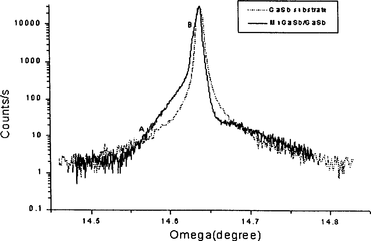
[0030] (1) Using GaSb single crystal as the substrate;

[0031] (2) Using an ion beam epitaxy system to epitaxially grow Ga with a graded composition on a GaSb substrate 1-x mn x Sb material;

[0032] (3) The samples were tested with the ω-2θ and small-angle diffraction modes of the X-ray diffractometer, and no new diffraction peaks were found in the test results. Ga 1-x mn x The ω-2θ diffraction curve (solid line) of the Sb sample along the (002) direction is shown in figure 1 shown. It can be calculated from the figure that the Mn content x gradually decreases from 0.09 to 0 from the surface to the inside of the crystal, and the corresponding lattice mismatch Δa / a 0 Gradually decrease from 0.005 to 0. Visible, Ga 1-x mn x The Sb sample is a semiconductor with a gradient composition of sphalerite structure;

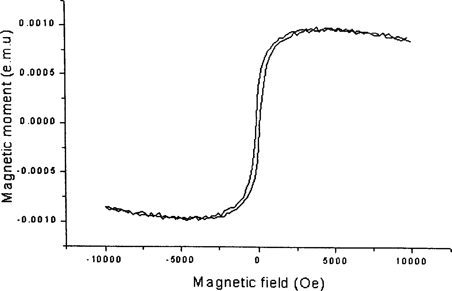
[0033] (4) At room temperature, the hysteresis loop of the above sample was measured with a vibrating sample magnetometer (VSM) LDJ9600 as figure 2 shown. w...


PUM

PropertyMeasurementUnit
Coercivityaaaaaaaaaa

Abstract

The preparation process of ferromagnetic semiconductor with graded components includes the first step of selecting semiconductor monocrystalline chip as substrate material; the second step of heatingthe substrate material; the third step of growing magnetic semiconductor material with graded components on the substrate; and the fourth step of heat treatment of the magnetic semiconductor material.

Description

technical field [0001] The invention relates to a method for preparing a ferromagnetic semiconductor film material, in particular to a method for preparing a composition-graded ferromagnetic semiconductor. Background technique [0002] Semiconductor materials and magnetic materials are two important types of materials that are indispensable in modern information technology, and semiconductor physics and magnetic physics are two branches of condensed matter physics. Combining magnetic properties with semiconductor properties to manufacture new functional devices is a very important branch of the development of magnetoelectronics. Therefore, it is very meaningful to magnetize existing semiconductor materials, both in terms of practical materials and fundamental physics. [0003] So far, a large number of magnet / semiconductor heterostructures and magnet / semiconductor / magnet triple-layer structures have been successfully prepared, and the development of magnet / semiconductor sup...

Claims


Application Information

Patent Timeline
IPC IPC(8): H01F1/40H01F41/00H01L21/00
Inventor 陈诺夫张富强杨君玲刘志凯杨少延柴春林
Owner INST OF SEMICONDUCTORS - CHINESE ACAD OF SCI
Why Eureka
Try Eureka