Process for making super-thin silicon nitride / silicon oxide grid electrode dielectric layer

A gate dielectric layer and manufacturing method technology, applied in the field of ultra-thin silicon nitride/silicon oxide gate dielectric layer manufacturing, can solve the problem of high process thermal budget, increase process complexity and instability, and reliable components sexual degeneration

Inactive Publication Date: 2003-12-31
TAIWAN SEMICON MFG CO LTD
View PDF0 Cites 10 Cited by
  • Summary
  • Abstract
  • Description
  • Claims
  • Application Information

AI Technical Summary

Problems solved by technology

Such an operation can reduce the defect density of the film, but the intensive annealing treatment not only increases the complexity and instability of the process, but also causes a high process thermal budget (Thermal Budget), and causes the impurities in the substrate to diffuse and cause component damage degrada

Method used


Image

  • Process for making super-thin silicon nitride / silicon oxide grid electrode dielectric layer
  • Process for making super-thin silicon nitride / silicon oxide grid electrode dielectric layer
  • Process for making super-thin silicon nitride / silicon oxide grid electrode dielectric layer

Examples


Embodiment Construction

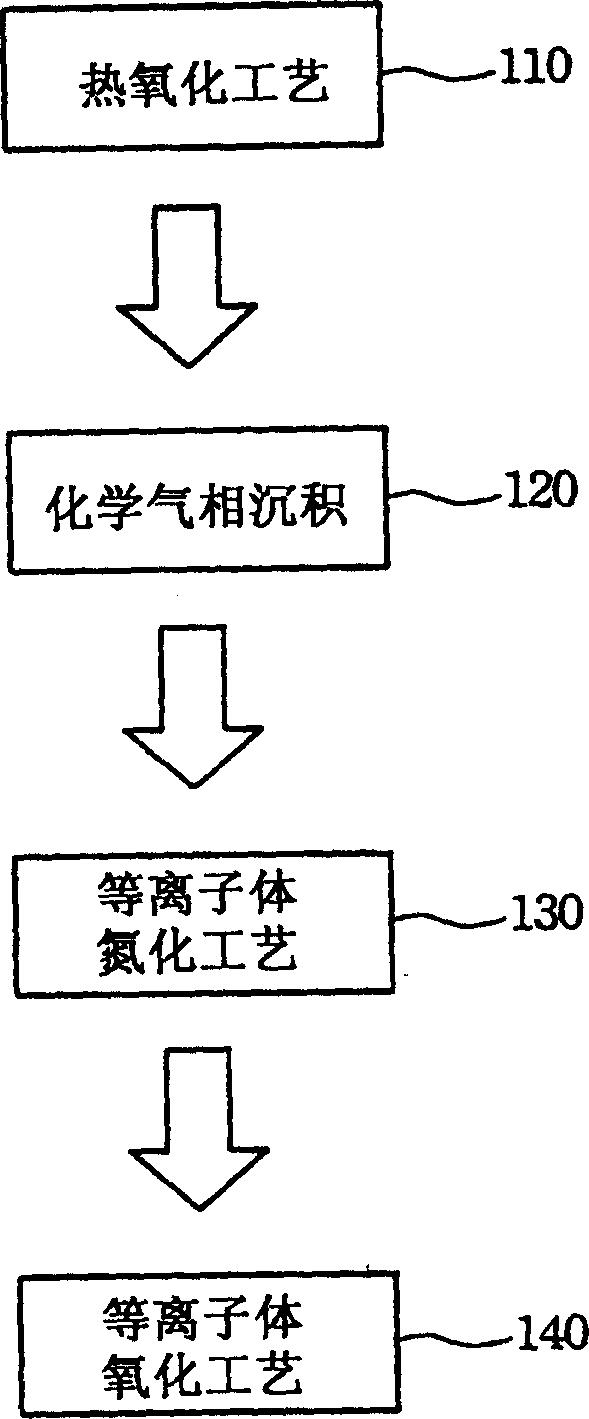
[0021] Due to the existing methods of manufacturing ultra-thin silicon nitride / silicon oxide gate dielectric layers in the background of the invention, an annealing treatment must be used to optimize the silicon nitride deposition process to reduce the defect density of the film. However, the annealing process causes the diffusion of impurities in the substrate, resulting in deterioration of device characteristics. Moreover, the multiple annealing processes of temperature rise and fall also increase the complexity and uncontrollability of the entire process, and further reduce the production capacity. Furthermore, the nitridation with ammonia gas further causes high concentration of hydrogen in the dielectric layer, which degrades the reliability of the device.

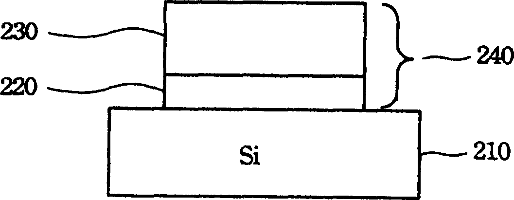
[0022] The invention provides a method for manufacturing an ultra-thin silicon nitride / silicon oxide gate dielectric layer, which utilizes N 2 Plasma nitriding process and O 2 or N 2 O plasma re-oxidation process t...


PUM


Abstract

The invention discloses a process for manufacturing ultra-thin silicon nitride / silicon oxide grid electrode dielectric layer, characterized by that, first forming a surface oxidation layer on a silicon substrate by silicon oxidation, then depositing silicon nitride layer on the surface oxidation layer, and nitrogenizing and oxidizing the silicon nitride using plasma body. The thermal oxidation silicon substrate is carried out by oxidizing the silicon substrate using oxygen or N#-[2]O, so as to form silicon oxide layer or silicon nitride layer. The deposition silicon nitride uses rapid heating chemical vapor deposition or remote plasma body to reinforce the chemical vapor deposition silicon nitride layer. Plasma body nitridation uses N#-[2] plasma body, and plasma body oxidation uses oxygen plasma body or N#-[2] plasma body to oxidizing the silicon nitride layer.

Description

technical field [0001] The invention relates to a method for manufacturing an integrated circuit gate dielectric layer, in particular to a method for manufacturing an ultra-thin silicon nitride / silicon oxide gate dielectric layer. Background technique [0002] As the size of integrated circuits shrinks to the deep submicron range, the need for gate oxide reliability becomes more and more urgent. This is because as the thickness of the gate oxide gradually shrinks, it rapidly approaches its limit due to high leakage currents induced by electron tunneling. Under the 0.1 micron technology, the thickness of the gate oxide layer must be reduced, and thinning the thickness of the gate dielectric layer is an effective method to control the short channel effect under the reduced gate width. The shrinking dimensions of integrated circuit components have increased the need for gate dielectrics with higher dielectric constants (compared to silicon dioxide). Such a requirement is extr...

Claims


Application Information

Patent Timeline
IPC IPC(8): H01L21/283H01L21/285H01L21/314
Inventor 陈启群李资良陈世昌
Owner TAIWAN SEMICON MFG CO LTD
Why Eureka
Try Eureka