
GaAs based composite collecting region trajectory transmitting heterojunction bipolar transistor

A heterojunction bipolar, gallium arsenide-based technology, applied in semiconductor devices, electrical components, circuits, etc., can solve problems such as breakdown voltage drop, device breakdown voltage drop, and device high breakdown voltage.

Inactive Publication Date: 2003-12-31
INST OF MICROELECTRONICS CHINESE ACAD OF SCI
View PDF0 Cites 4 Cited by
  • Summary
  • Abstract
  • Description
  • Claims
  • Application Information

AI Technical Summary

Problems solved by technology

However, its breakdown voltage decreases as the thickness of the collector region decreases
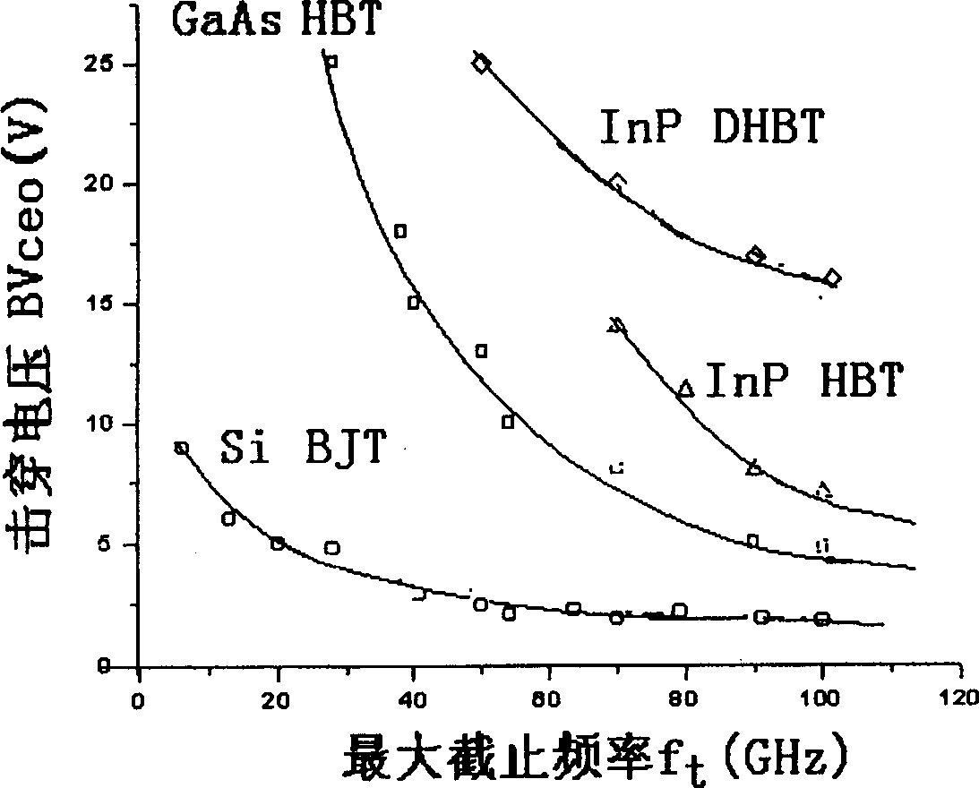
However, in many microwave and millimeter wave circuits (such as optical modulator drive circuits), not only the device is required to have a high cut-off frequency, but also the device is required to have a high breakdown voltage
while the above and figure 1 It can be seen that increasing the cut-off frequency of the device and increasing the breakdown voltage are contradictory
Reducing the thickness of the collector region can reduce the transit time of electrons in the depletion region of the collector junction and increase the cut-off frequency of the device, but this will reduce the breakdown voltage of the device

Method used


Image

  • GaAs based composite collecting region trajectory transmitting heterojunction bipolar transistor
  • GaAs based composite collecting region trajectory transmitting heterojunction bipolar transistor
  • GaAs based composite collecting region trajectory transmitting heterojunction bipolar transistor

Examples


Embodiment Construction

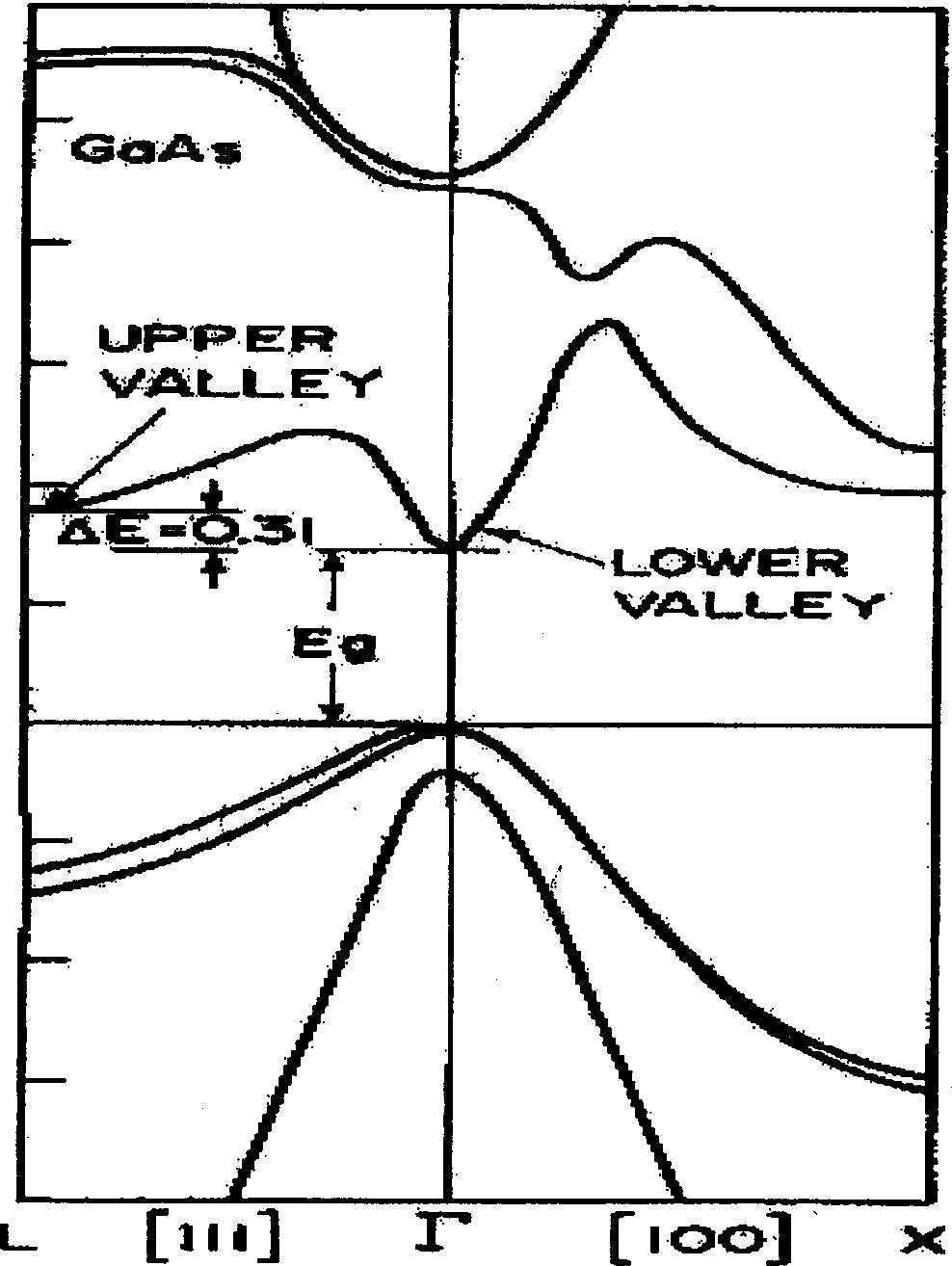
[0017] In GaAs, the difference between the Γ energy valley and the L energy valley is 0.31eV, such as figure 2 shown. Under the action of a strong electric field, the electrons in the Γ energy valley jump to the L energy valley, which reduces the speed of electron movement. After the electron reaches the L energy valley, it will be 8×10 6 cm / s saturation velocity motion. However, the transient process is accompanied by changes in electron momentum and energy. Under a strong electric field, since the momentum relaxation time is shorter than the energy relaxation time, the time required to complete the transient is on the order of the energy relaxation time. In GaAs electrons exist 10 before the transition to the L energy valley -13 -10 -12 seconds energy relaxation time, during the energy relaxation time, there is an overshoot phenomenon in the speed of electrons, and the overshoot speed is as high as 5×10 7 cm / s, electrons must travel a certain distance in the gamma ener...


PUM


Abstract

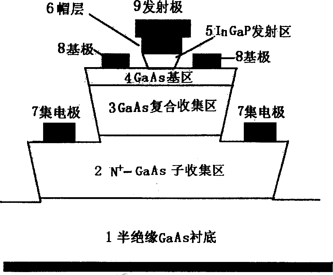
The invention discloses a GaAs based composite collecting region trajectory transmitting heterojunction bipolar transistor comprising, a semi-insulating GaAs substrate, a N#+[+] adulterated GaAs collecting sub-region grown on the semi-insulating GaAs substrate, a composite collecting region grown on the N#+[+] adulterated GaAs collecting sub-region, a heavy type P GaAs base grown on the composite collecting region. On the base region a type N InGaP emitting region is formed the top of which is a cap layer used for making Ohm contact, an emitting electrode is formed on the cap layer, and a base electrode is formed on the type N InGaP emitting region on the base region.

Description

Technical field: [0001] The invention belongs to the field of semiconductor microelectronics and microwave devices, in particular to a gallium arsenide-based compound collection area ballistic transmission heterojunction bipolar transistor. Background technique [0002] Due to the superior high-frequency, high-speed and high-current driving capabilities of the heterojunction bipolar transistor (HBT), it has great application potential in digital, analog and power amplifiers. At present, there are mainly three material systems—germanium silicon (GeSi), gallium arsenide (GaAs) and indium phosphide (InP)—for the preparation of HBT. All three material systems can be applied in the microwave and millimeter wave fields. GaAs HBT has broad application prospects in microwave and millimeter wave fields due to its high reliability and relatively mature technology. At present, GaAs HBT and its related circuits are still the most researched and most widely used in the market. [0003...

Claims


Application Information

Patent Timeline
IPC IPC(8): H01L29/737
Inventor 石瑞英刘训春
Owner INST OF MICROELECTRONICS CHINESE ACAD OF SCI
Learn More