Polyimide resin precursor solution, laminates for electronic components made by using the solution and process for production of the laminates
A technology of polyimide resin and precursor solution, applied in circuit substrate materials, printed circuit parts, conductive layers on insulating carriers, etc., can solve the problems of metal ion migration and loss of resin insulation, etc.
- Summary
- Abstract
- Description
- Claims
- Application Information
AI Technical Summary
Problems solved by technology
Method used
Image
Examples
Embodiment 1
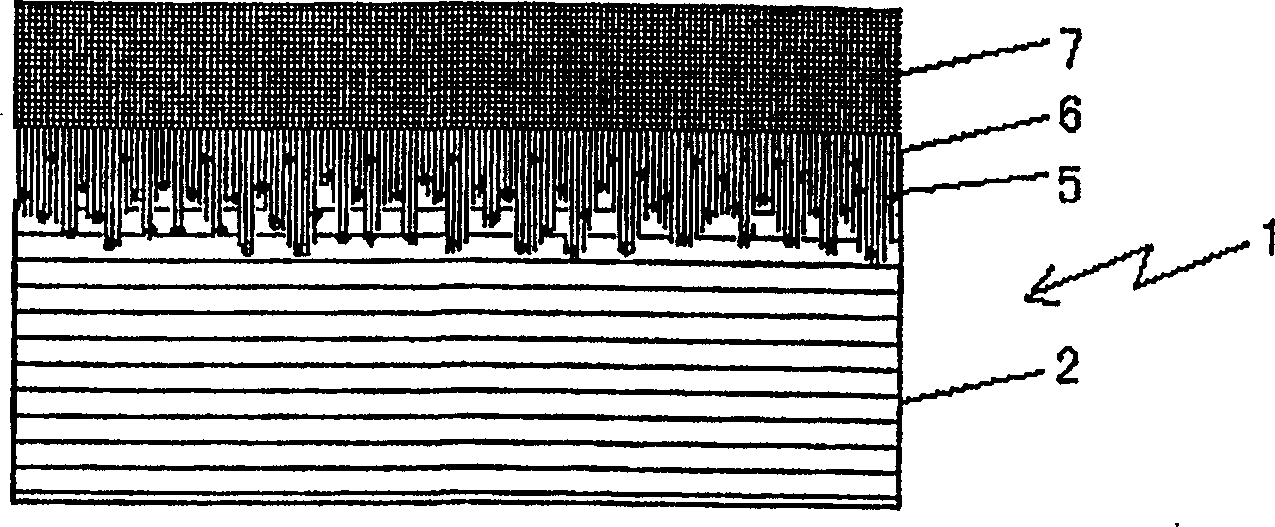
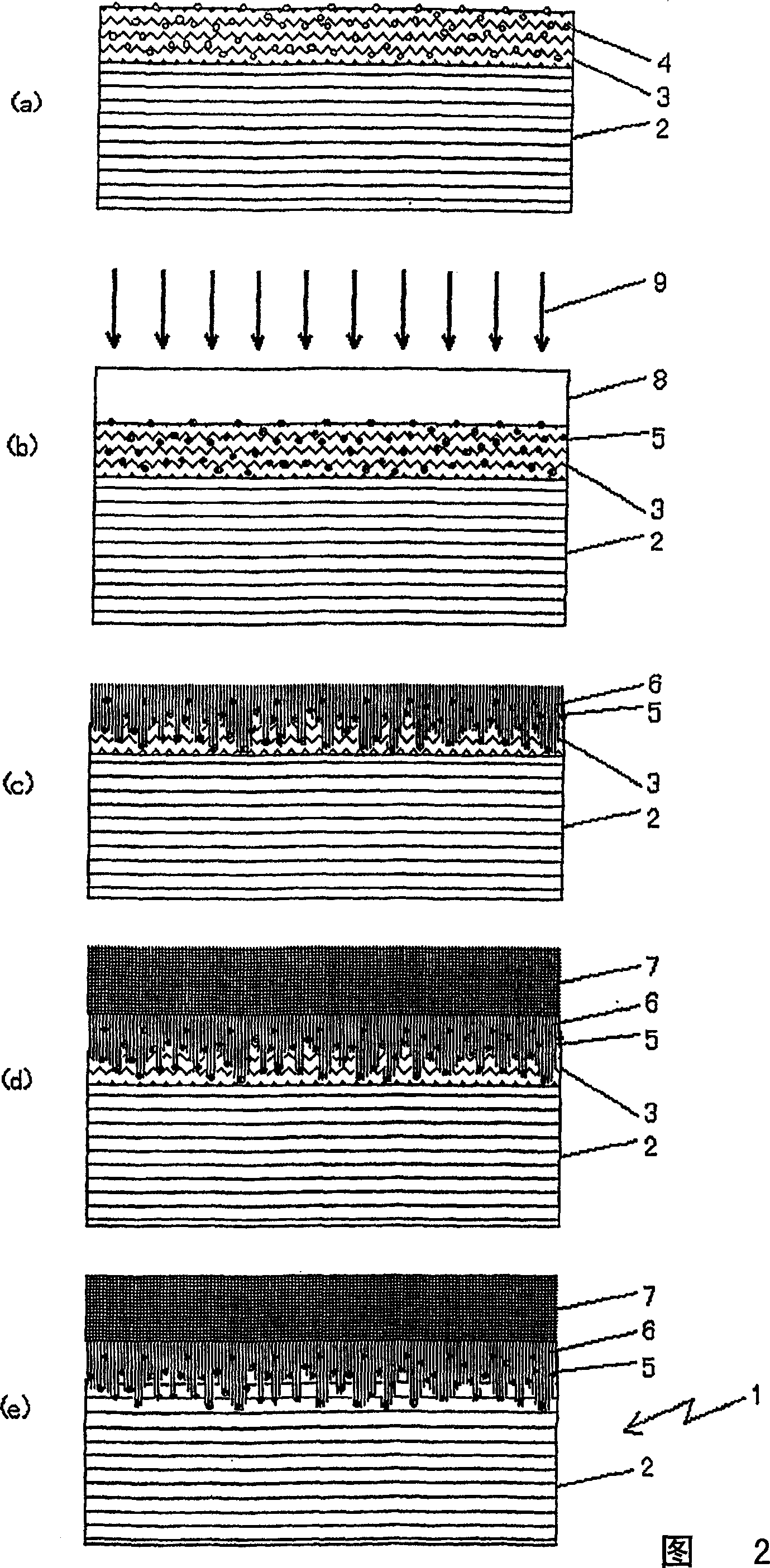
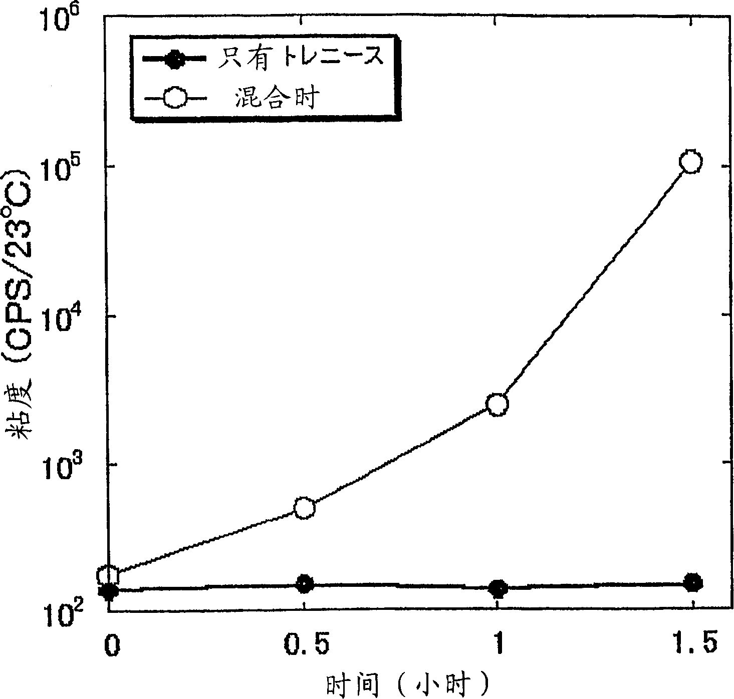
[0052] A solution of a commercially available palladium acetylacetone complex (hereinafter referred to as palladium complex) dissolved in N-methyl-2-pyrrolidone (hereinafter referred to as NMP) was added to the polyimide of Toray Co., Ltd. In the amine resin precursor varnish "トレニ-ス" #3000, the varnish solution was adjusted so that the average content of the palladium complex compound in the varnish solution became 1 wt / vol%. The varnish solution contains an average polyimide resin precursor of approximately 5 wt / vol% of the palladium coordination compound.
[0053] In addition, the so-called 1 wt / vol% refers to, for example, the concentration of 0.01 g of the palladium complex compound dissolved in 1 ml of "Toraynis" varnish solution.
[0054] Next, a test piece of 10×10 cm (thickness 50μm) of the polyimide substrate "Yu-ピレツクス-S" from Ube Industries Co., Ltd. was treated with 1% NaOH aqueous solution and 1% HCl aqueous solution, and washed with pure water. After drying, the varni...
Embodiment 2
[0061] The palladium complex content of the polyimide resin precursor solution of Example 1 was changed to 0.5 wt / vol%, and the same treatment was performed to prepare a substrate for electronic parts with a copper film thickness of 22 μm. As a result of measuring the peel strength between the metal portion of the obtained substrate and the polyimide resin layer by the method specified in JISC-6481, it was 12 N / cm (1200 gf / cm).
Embodiment 3
[0063] Change the ultraviolet radiation dose of Example 1 to 7500mJ / cm 2 , Proceed with the same treatment.
PUM
| Property | Measurement | Unit |
|---|---|---|
| Thickness | aaaaa | aaaaa |
| Peel strength | aaaaa | aaaaa |
| Film thickness | aaaaa | aaaaa |
Abstract
Description
Claims
Application Information


