Device and method for growng large diameter 6H-SiC monocrystal with semiconductor property

A growth method and large-diameter technology, applied in the field of crystal growth, can solve the problems that limit the development process of silicon carbide crystals and devices, and achieve the effect of large diameter

Active Publication Date: 2004-12-15
SICC CO LTD
View PDF0 Cites 39 Cited by
  • Summary
  • Abstract
  • Description
  • Claims
  • Application Information

AI Technical Summary

Problems solved by technology

Calculations have shown that in order to grow single crystals directly from silicon carbide melts by Czochralski or zone melting methods like silicon or gallium arsenide, in order to maintain the 1:1 ratio of carbon to silicon in the melt, it is necessary to create 3200 The harsh conditions of high temperature above 100,000 ℃ and high pressure above 100,000 atmospheres were a natural obstacle at that time and even now, limiting the development of silicon carbide crystals and device industrialization.

Method used


Image

  • Device and method for growng large diameter 6H-SiC monocrystal with semiconductor property
  • Device and method for growng large diameter 6H-SiC monocrystal with semiconductor property
  • Device and method for growng large diameter 6H-SiC monocrystal with semiconductor property

Examples


Embodiment 1

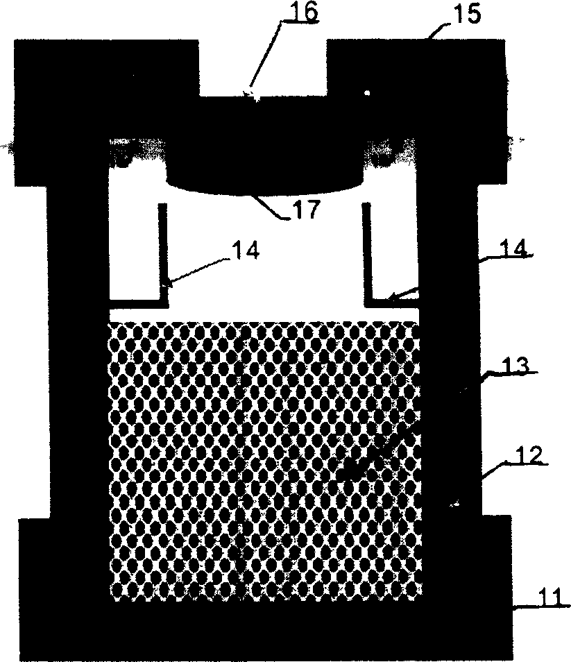
[0036] Embodiment 1. The device of the large-diameter 6H-SiC single crystal of growth semiconductor characteristic, structure such as figure 1 and 2 shown.

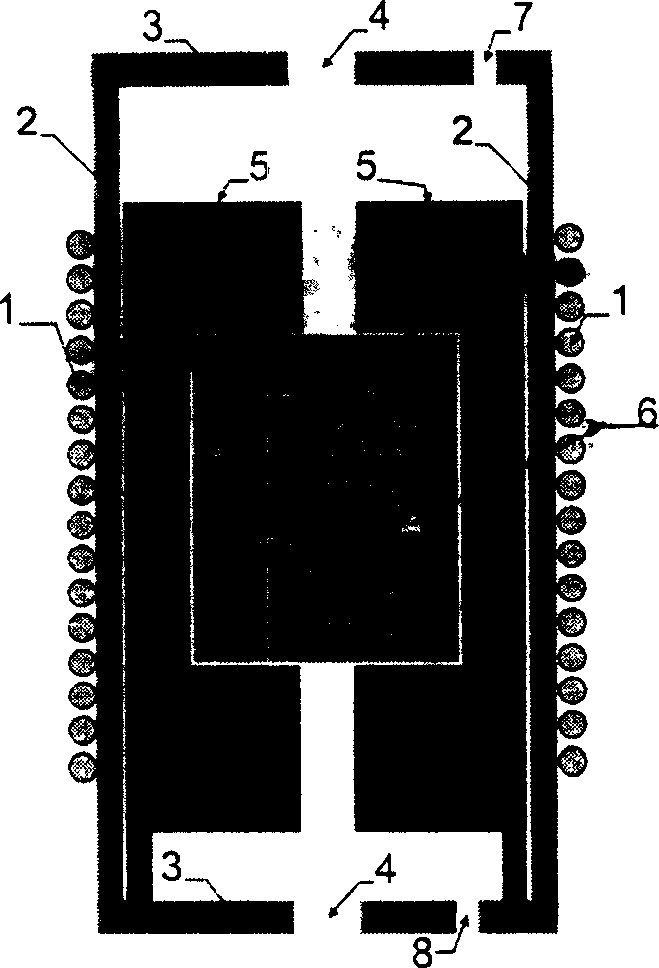
[0037] The graphite crucible 6 is placed in the growth chamber. The top of the crucible has a seed crystal seat 16 that can fix the seed crystal, the bottom holds SiC powder 13, and a built-in cylindrical gas phase deflector 14, thereby achieving the purpose of controlling the transport of SiC species . There is a gas port 7 on the upper part of the growth chamber, through which gas enters the growth chamber during the growth process. There is a gas outlet 8 in the lower part of the growth chamber, and vacuum conditions are used to remove harmful substances such as oxygen and water; gas is introduced to provide the atmosphere and pressure required for crystal growth. The upper and lower parts of the growth chamber are hermetically connected by stainless steel flange sealing ring 3 and quartz double-layer glass tube 2, ...

Embodiment 2

[0038] Embodiment 2. A device for growing large-diameter 6H-SiC single crystals with semiconductor characteristics: as described in Embodiment 1, the difference is that there is a built-in cylindrical gas phase deflector 14 and a circular concave crucible wall 12 in the crucible. crystals grown as Figure 4 As shown, the region indicated by the arrow at the end of the crystal grows freely, indicating that the gas phase deflector can effectively control the sublimation and diffusion of the growing species.

Embodiment 3

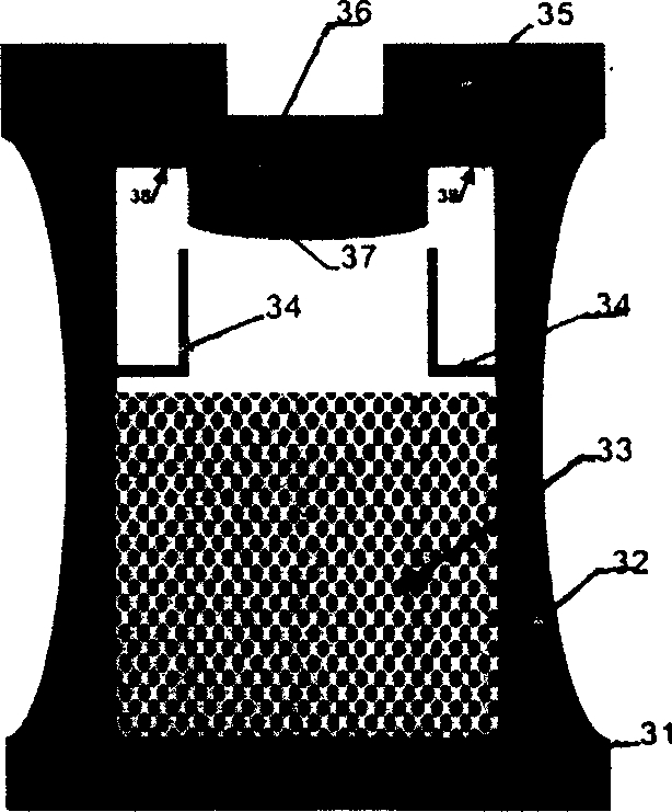
[0039] Embodiment 3. The device for growing a large-diameter 6H-SiC single crystal with semiconductor characteristics: as described in Embodiment 1, the difference is that the side wall of the crucible is an arc-shaped curve 32, such as image 3 shown.


PUM

PropertyMeasurementUnit
densityaaaaaaaaaa
particle sizeaaaaaaaaaa

Abstract

The present invention relates to apparatus and method of growing great diameter 6H-SiC monocrystal with semiconductor characteristic and belongs to the field of crystal growing technology. The apparatus includes growing chamber, water cooler on the side wall of the growing chamber, graphite crucible, heat insulating material, induction heating system, cylindrical vapor guiding plate of Ta inside the crucible, and cylinder. Regulating the position of the crucible relative to the inducing coil can minimize the temperature at the crystal seed inside the crucible and increase the temperature field distribution in the growing direction. Altering the atmosphere composition or material compounding can obtain great diameter SiC monocrystal with n-type, p-type or semi-insulating type semiconductor characteristic. By means of selecting the Si plane of the crystal seed and growing temperature, the crystal form may be controlled and 6H-SiC may be obtained.

Description

(1) Technical field [0001] The invention relates to a device and method for growing a 6H-SiC single crystal with semiconductor characteristics and a diameter not less than 2 inches, belonging to the technical field of crystal growth. (2) Background technology [0002] Silicon carbide is famous for its high hardness (second only to diamond). Its powder is widely used in abrasives and abrasive tools for machining. The history of artificial synthesis can be traced back to the 19th century. However, the growth of SiC single crystals is particularly difficult. Although there have been more than 50 years of single crystal growth history, the crystal quality and size still cannot meet the device requirements. SiC single crystal has a wide band gap and is often called the third-generation wide-bandgap semiconductor material. It has high thermal conductivity, 20 times that of sapphire, high carrier saturation drift velocity, and low dielectric constant. , can be used to prepare high...

Claims


Application Information

Patent Timeline
Patent Type & Authority Applications(China)
IPC IPC(8): C30B23/00C30B29/36
Inventor 徐现刚胡小波王继扬王丽蒋民华
Owner SICC CO LTD
Why Eureka
Try Eureka