Prepn. of inner chanber contacting vertical chamber emitting laser by 3-shaft self-aligning process

A vertical cavity surface emission and self-alignment technology, which is applied in the field of VCSEL manufacturing process, can solve the problems of low lithography precision and non-repeatable complete alignment of three axes, so as to increase the number of lithography times and reduce the lithography precision the effect of the requirements

Inactive Publication Date: 2005-01-12
BEIJING UNIV OF TECH
View PDF0 Cites 4 Cited by
  • Summary
  • Abstract
  • Description
  • Claims
  • Application Information

AI Technical Summary

Problems solved by technology

[0007] The purpose of the present invention is to provide a process flow for preparing an intracavity contact vertical cavity surface emitting laser by a three-axis self-alignment method. Accurate vertical-cavity surface-emitting laser devices solve the problem of three-axis non-repeatable complete alignment existing in the current fabrication of vertical-cavity surface-emitting laser devices, improve production efficiency, and reduce production costs

Method used


Image

  • Prepn. of inner chanber contacting vertical chamber emitting laser by 3-shaft self-aligning process
  • Prepn. of inner chanber contacting vertical chamber emitting laser by 3-shaft self-aligning process
  • Prepn. of inner chanber contacting vertical chamber emitting laser by 3-shaft self-aligning process

Examples


Embodiment Construction

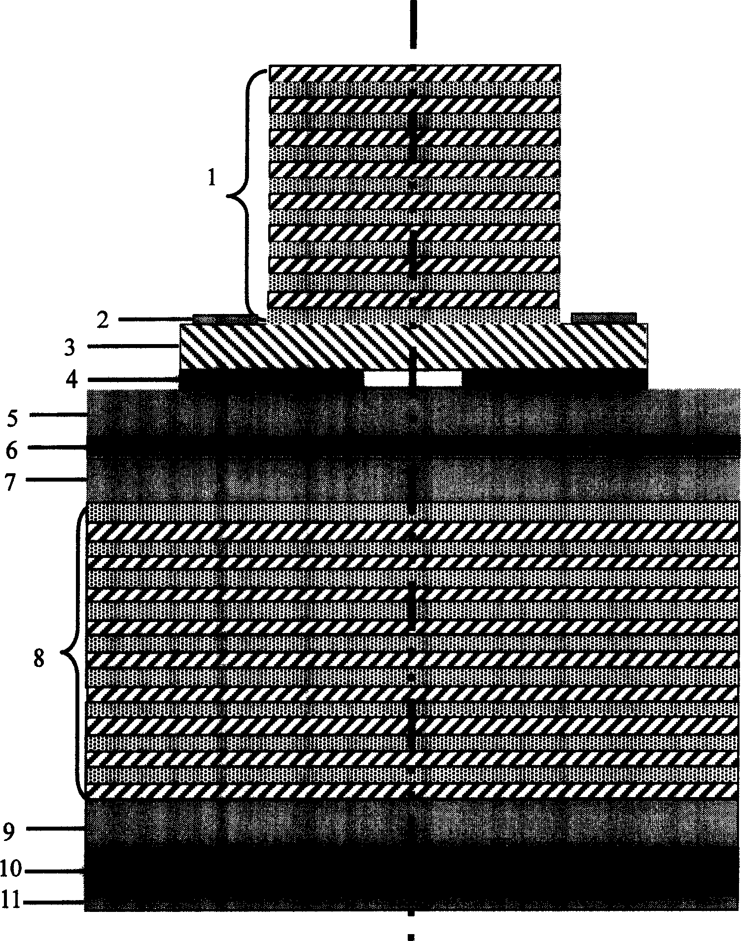
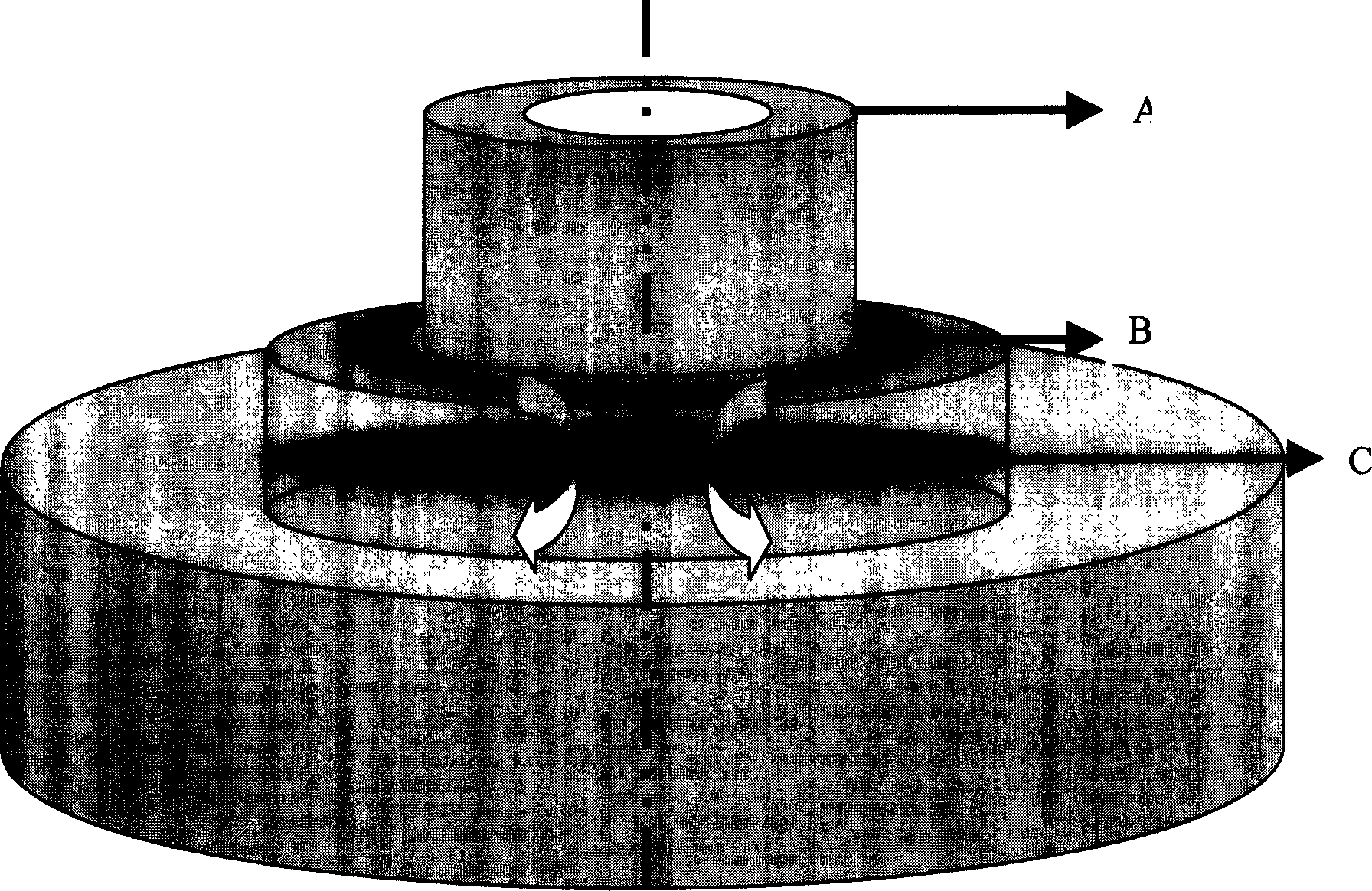
[0040] Such as Figure 3-1 Shown in ~9, its preparation process and method are as follows:

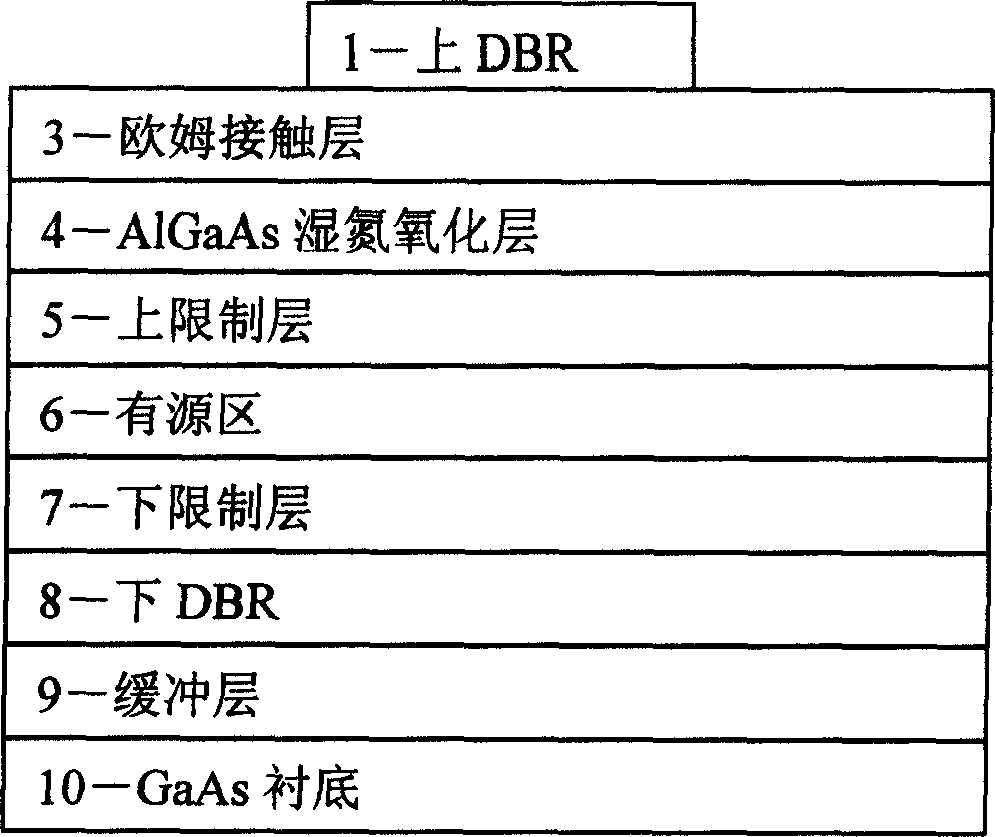
[0041] 1. Using common metal-organic chemical vapor deposition (MOCVD) method in n + -GaAs buffer layer 9, 28 pairs of 70nm GaAs / 80nm Al are epitaxially grown sequentially on GaAs substrate 10 0.9 Ga 0.1 Distributed Bragg Reflector 8 under As, 110nm Al x Ga 1-x As (xx Ga 1-x As(x0.98 Ga 0.02 As wet oxynitride layer 4, 100nm GaAs ohmic contact layer 3, 20 pairs of 70nmGaAs / 80nm Al 0.9 Ga 0.1 Distributed Bragg reflector 1 on As, where GaAs and Al 0.9 Ga 0.1 As are two materials constituting the upper and lower distributed Bragg reflectors respectively.

[0042] 2. Using Karl Suss BJ3 photolithography machine, and positive photoresist PR4200 photoresist, after exposure and development, the surface of the MOCVD growth sample is formed as Figure 3-1 The photoresist pattern shown.

[0043] 3. Using traditional dry etching technology (such as ICP or RIE) or wet chemical etching tec...


PUM


Abstract

Following steps are carried out by using traditional technique: photo etching from up distributed Bragg reflector to ohmic contact layer in dual groove shape; depositing P type ohmic contact electrode Ti/Pt/Au; peeling off procedure reserves Ti/Pt/Au on ohmic contact layer only; etching down no mask protected up distributed Bragg reflector, ohmic contact layer and AlxGa1-xAs(x is greater than or equal to 0.9) wet nitrogen oxidation respectively in registration photoetching procedure by using photoresist and P type ohmic contact electrode Ti/Pt/A as masks; Removing photoresist, wet nitrogen oxidating forming oxidation aperture; n type ohmic contact electrode obtained after thinning and polishing. Disclosed method obtains product by using photoetching device in low precision.

Description

Technical field: [0001] A vertical cavity surface emitting laser (VCSEL) prepared by a three-axis self-alignment method belongs to the technical field of semiconductor optoelectronics and relates to a VCSEL preparation process. Background technique: [0002] Due to its unique physical structure, the vertical cavity surface emitting laser (VCSEL) has the advantages of large longitudinal mode spacing, circular light spot, easy coupling with optical fiber, and easy formation of two-dimensional arrays. It plays an important role in optical communication, optical interconnection, and optical computing. play an increasingly important role. [0003] Vertical cavity surface emitting lasers are usually mainly composed of upper and lower distributed Bragg reflectors (DBR) and an active region sandwiched in the middle, in which the distributed Bragg reflectors are periodically composed of two or more semiconductor or dielectric materials with different refractive indices. Alternate gr...

Claims


Application Information

Patent Timeline
Patent Type & Authority Applications(China)
IPC IPC(8): H01S5/183
Inventor 郭霞沈光地杜金玉邹德恕
Owner BEIJING UNIV OF TECH
Why Eureka
Try Eureka