Amorphous crystallization preparation method for nano crystal thermoelectric semiconductor material

A thermoelectric semiconductor and nanocrystalline technology, applied in the field of new energy materials, can solve the problems of easy introduction of other impurities, uneven grain size, difficulty in obtaining high-purity thermoelectric semiconductor materials, etc. The effect of easy large-scale preparation

Inactive Publication Date: 2005-03-16
WUHAN UNIV OF TECH
View PDF0 Cites 7 Cited by
  • Summary
  • Abstract
  • Description
  • Claims
  • Application Information

AI Technical Summary

Problems solved by technology

[0004] At present, nanocrystalline thermoelectric semiconductor materials are mainly prepared by high-energy ball milling combined with certain sintering methods. The main disadvantages o

Method used


Image

  • Amorphous crystallization preparation method for nano crystal thermoelectric semiconductor material

Examples


Example Embodiment

[0021] Example 1: Bulk CoSb 3 Preparation of Nanocrystalline Thermoelectric Semiconductor Material

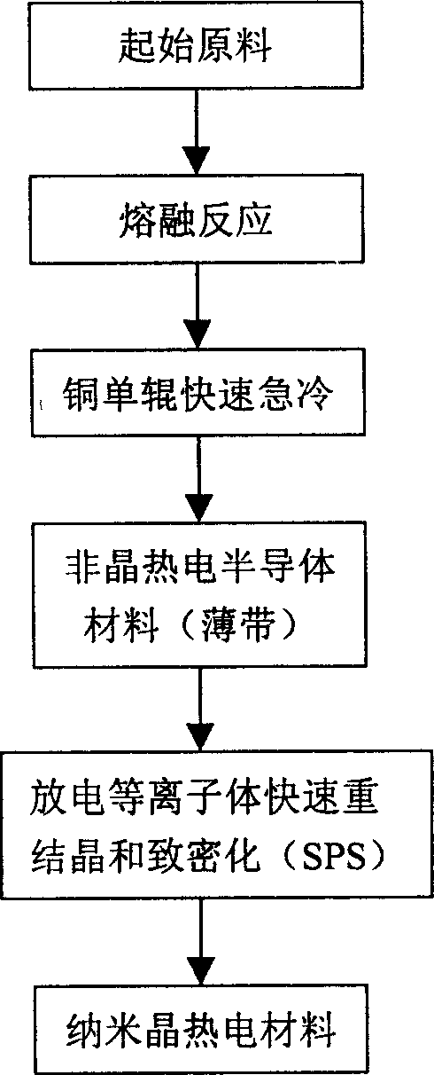
[0022] Using cobalt powder and antimony powder as raw materials, melt reaction at 1100℃ to obtain uniform CoSb 3 Melt, using copper single copper roll quenching technology, to 10 5 Preparation of CoSb at a cooling rate of ℃ / sec 3 The amorphous alloy strip has a width of about 2 to 3 mm, a thickness of about 25 μm, a length of several meters, and a smooth surface.

[0023] The strips weighing about 5g are ground and pulverized into powder, and then packed into a graphite mold of φ10mm for compaction, and then moved together with the mold into the spark plasma rapid recrystallization and densification sintering (SPS) equipment. The vacuum degree in the furnace is 10 -3 Pa, heat up to 600℃ for recrystallization, use 30MPa pressure for densification, recrystallization and densification time is 7min, after cooling, take out the mold and get a block material with a diameter of 10mm and a...

Example Embodiment

[0024] Example 2: Bulk Ba is filled with nano-skutterudite compound Ba y Co 4 Sb 12 Preparation of thermoelectric semiconductor materials

[0025] Using bulk barium, cobalt powder and antimony powder as raw materials, the melting reaction is carried out at 1100°C to obtain uniform Ba-filled Ba y Co 4 Sb 12 Melt, using copper single copper roll quenching technology, to 10 5 ℃ / sec cooling rate to prepare Ba y Co 4 Sb 12 The amorphous alloy strip has a width of about 2 to 3 mm, a thickness of about 25 μm, a length of several meters, and a smooth surface.

[0026] The strips weighing about 8g are ground and crushed into powder, and then packed into a φ20mm graphite mold for compaction, and then moved together with the mold into the spark plasma rapid recrystallization and densification sintering (SPS) equipment. The vacuum in the furnace is 10 -3 Pa, heat up to 600℃ for recrystallization, and use 30MPa pressure for densification. The recrystallization and densification time is 8min. A...


PUM

PropertyMeasurementUnit
Diameteraaaaaaaaaa
Average grain sizeaaaaaaaaaa

Abstract

A nanocrystalline thermoelectric semiconductor material amorphous crystallization production method is provided, compriseing the stepss of: first adopting high-frequency heating and obtaining uniform alloy melt at 1100 DEG C, then cooling smelt to get thin strip or filament shaped amorphous sample using liquid phase quenching method, cooling speed being 10<5>-10<6> DEG C/sec, grinding amorphous sample and place in mould, placing mould in discharge plasm fast recrystallization and densification sintering apparatus, recrystallization and densification temperature being 600 DEG C, pressure 30Mpa,time 7-8min, obtaining high purity, average mean crystal grain size 70-80nm,uniform crystalline grain, high performance block nanocrystalline thermoelectric semiconductor material. The invention provides a technology for scale preparation of block nanocrystalline thermoelectric semiconductor material.

Description

technical field [0001] The invention relates to a preparation method of a nanocrystalline thermoelectric semiconductor material, which belongs to the field of new energy materials. Background technique [0002] As a new type of energy conversion technology in the 21st century, thermoelectric conversion technology is used as thermoelectric power generation and thermoelectric cooling devices in military, medical , Civil and other aspects have broad application prospects. Especially with the increasingly serious environmental problems and energy problems, thermoelectric conversion technology shows great potential in the conversion and utilization of solar energy and the application as a micro power system. The key to the practical application of thermoelectric conversion technology is the research and development of high-performance thermoelectric semiconductor materials. [0003] When the microscale of thermoelectric semiconductor materials decre...

Claims


Application Information

Patent Timeline
IPC IPC(8): C22C1/04C22C12/00C22C19/07
Inventor 唐新峰宋波熊聪刘桃香张清杰
Owner WUHAN UNIV OF TECH
Why Eureka
Try Eureka