
Nano-beam resonator with field effect pipe manufactured using sacrifice layer corrosion technology

A field effect tube and resonator technology, applied in the direction of nanotechnology, nanotechnology, nanostructure manufacturing, etc., to achieve the effects of cost reduction, good promotion and application range, and simple manufacturing process

Inactive Publication Date: 2005-05-25
ZHEJIANG UNIV
View PDF0 Cites 7 Cited by
  • Summary
  • Abstract
  • Description
  • Claims
  • Application Information

AI Technical Summary

Problems solved by technology

Another differential detection method similar to the Wheatstone bridge, because the signal and the driving voltage are at the same frequency, there are certain problems in the occasions where the contrast requirements such as analysis noise are relatively high.

Method used


Image

  • Nano-beam resonator with field effect pipe manufactured using sacrifice layer corrosion technology
  • Nano-beam resonator with field effect pipe manufactured using sacrifice layer corrosion technology

Examples


Embodiment Construction

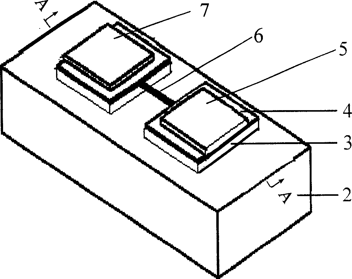
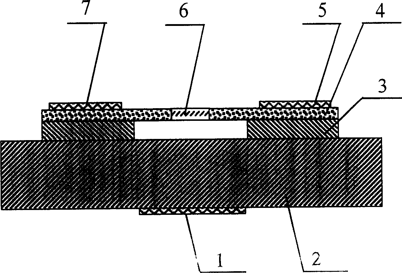
[0009] refer to figure 1 , figure 2 , the present invention uses SOI silicon epitaxial wafers as raw material and is manufactured by micro-nano machining process. Cantilever nano-beam 6 is manufactured using photoresist as a mask, using Reactive Ion Etching (Reactive Ion Etching) process to etch silicon dioxide insulating layer 3 between silicon layer 4 and SOI, and then using sacrificial layer etching technology to etch the nano-beam The silicon dioxide insulating layer 3 beneath the beam 6 is hollowed out. The side walls of the cantilever nano-beam 6 fabricated by this process are vertical. The manufacture of P-i-P or N-i-N channel structure is to use photoresist as a mask to photoetch out the region to be doped, and then perform boron or phosphorus implantation to form P + or N + area.

[0010] The specific production process is described as follows:

[0011] 1. Using SOI silicon epitaxial wafers as raw materials, they are cut and cleaned to make standard silicon epi...


PUM


Abstract

A nanobeam resonator with FET is prepared by sacrifice layer etching process, and is composed of nanobeam resonator and its metallic electrodes. Said etching process includes such steps as preparing the nanobeam on the silicon layer on the insulating material (SOI), doping B or P to both ends of nanobeam to form P-i-P or N-i-N channel structure used as the channel of FET, and using the bottom electrode as the grid of FET.

Description

technical field [0001] The invention relates to a resonator, especially a nano-beam resonator. Background technique [0002] The nanobeam resonator is a very typical nanoelectromechanical system (Nano Electromechanical System, NEMS) device. It can not only be directly applied in radio frequency circuits as radio frequency filters, oscillators, frequency reference components, etc., but also many sensors are based on resonators, such as resonant sensors, gyroscopes, etc. In Micro Electromechanical System (NEMS, MEMS) devices, many excitation and detection methods suitable for MEMS devices have been developed, such as electromagnetic, electrostatic, piezoresistive, laser and so on. But for a nano-beam resonator, because the volume is too small, the excitation and detection methods commonly used in MEMS devices will no longer be suitable for the nano-beam resonator. The detection methods currently used for nanobeam resonators, such as electromagnetic detection assisted by stro...

Claims


Application Information

Patent Timeline
IPC IPC(8): B82B1/00B82B3/00H01L21/335H01L29/772H03H9/00
Inventor 金仲和马慧莲鲍景富丁纯王跃林
Owner ZHEJIANG UNIV
Learn More