Preparation method of gallium adulterated zinc oxide transparent conductive film
A technology of transparent conductive film and transparent conductive film, applied in metal material coating process, vacuum evaporation plating, coating and other directions, can solve problems such as unfavorable film growth and poor heat bearing capacity, save precious metal indium, adhere to Good performance and wide application range
- Summary
- Abstract
- Description
- Claims
- Application Information
AI Technical Summary
Problems solved by technology
Method used
Image
Examples
Embodiment 1
[0031] Example 1: Preparation of gallium-doped zinc oxide transparent conductive film material by biased radio frequency magnetron sputtering technology.
[0032] The composition of the ceramic target for sputtering is: 1 part of ZnO, Ga 2 O 3 0.03 parts are all mole parts. ZnO and Ga 2 O 3 After the powder raw materials are ball milled for 2 hours and mixed uniformly, they are rolled into a billet with a hydraulic press at a pressure of 60Mpa, and then sintered at 1200°C for 2 hours, then charged to 800°C, and cooled naturally after turning off the power.
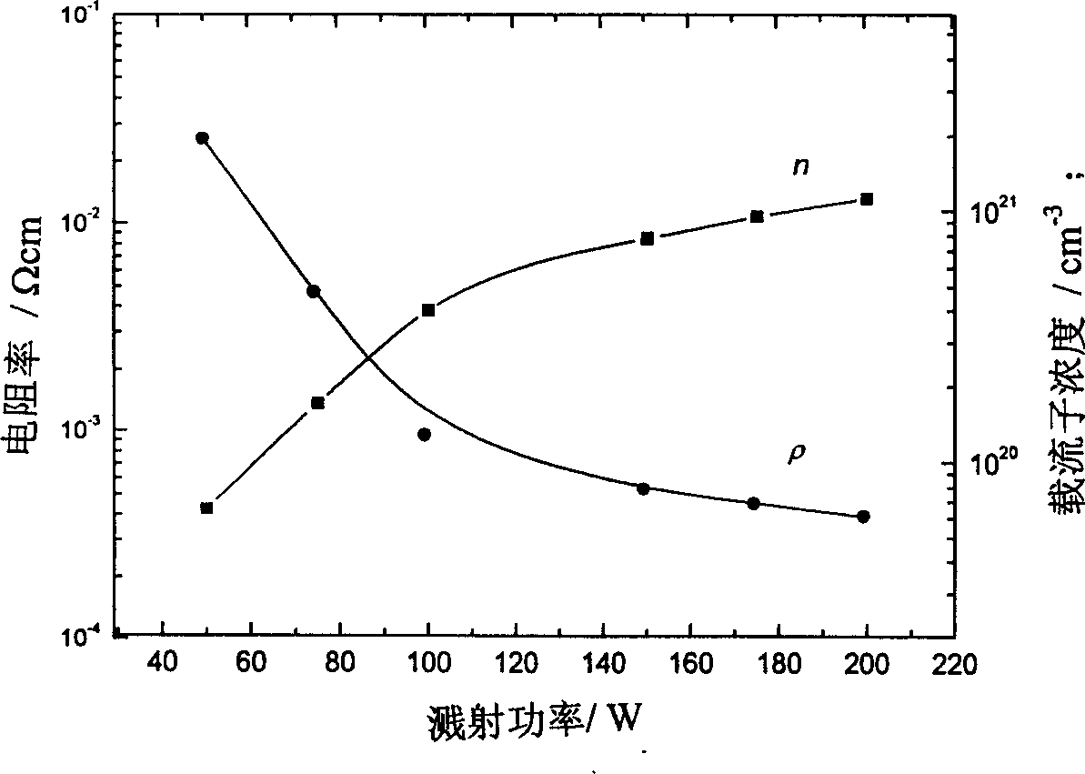
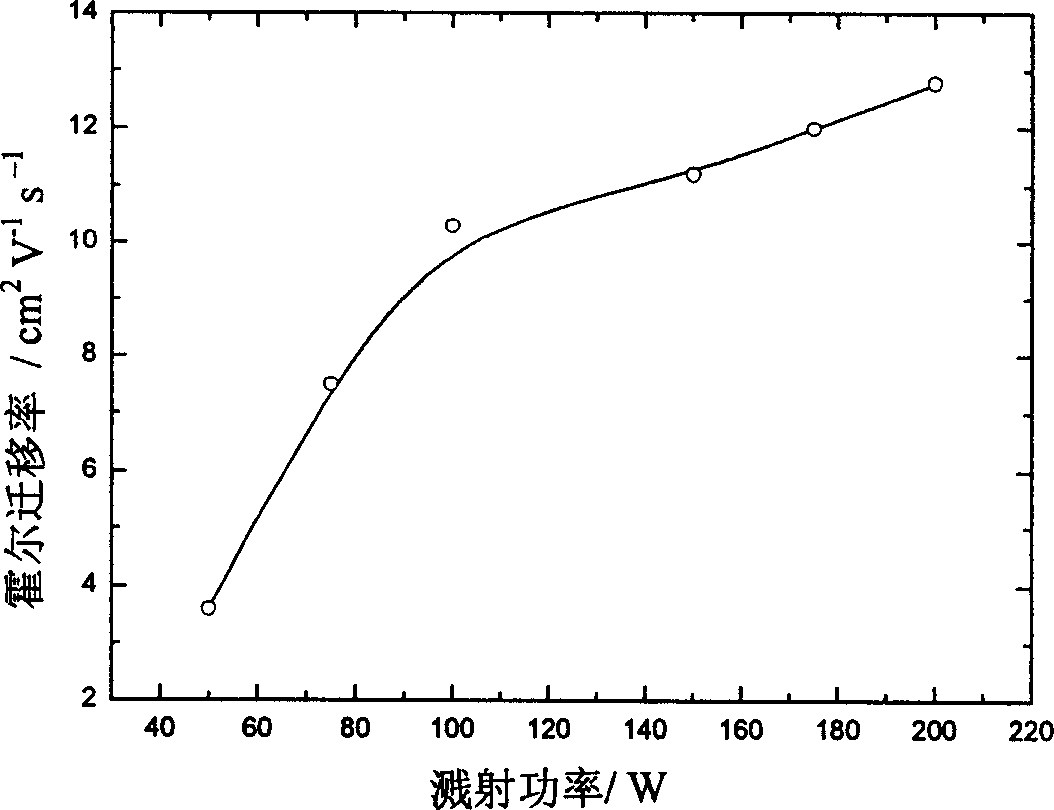
[0033] Polypropylene ethylene glycol (PPA) film is used as the substrate material, the diameter of the target is 6.5 cm, and the distance from the target to the substrate is 5 cm. The ZnO:Ga transparent conductive film prepared under the conditions of argon partial pressure 2Pa, sputtering power 150W, bias voltage 0V, and substrate temperature at room temperature is a polycrystalline film, the growth rate of the film is 19nm / m...
Embodiment 2
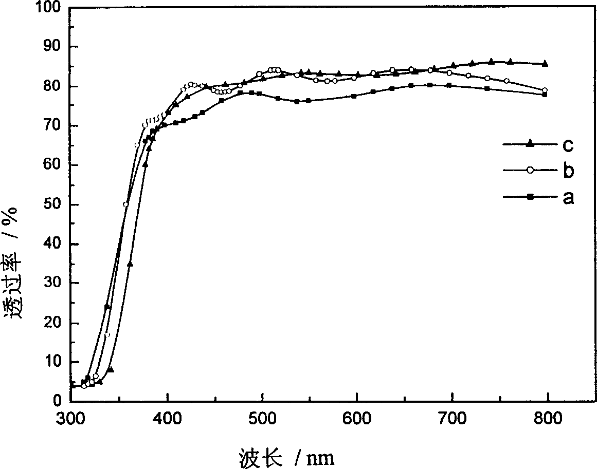
[0035] The ZnO:Ga transparent conductive film material was prepared by the biased radio frequency magnetron sputtering technology, and the composition of the ceramic target for sputtering was the same as that of Example 1. Polypropylene ethylene glycol (PPA) film is used as the substrate material. The ZnO:Ga transparent conductive film is a polycrystalline film prepared under the conditions of argon partial pressure 1Pa, sputtering power 150W, bias voltage -75V, and substrate temperature at room temperature. The growth rate of the film is 21nm / min, and the resistivity of the film is 4.6×10 -4 Ωcm, sheet resistance 6.2Ω / □, and the average relative transmittance in the visible light range exceeds 83%.
Embodiment 3
[0037] The composition of the ceramic target for sputtering is 1 part of ZnO, Ga 2 O 3 , 0.05 parts, all molar parts, the ceramic target preparation method is
[0038] Example 1 is the same.
[0039] The substrate material is a polyethylene terephthalate film, and the film preparation conditions are the same as in Example 2. The obtained ZnO:Ga transparent conductive film has a polycrystalline structure, and the resistivity of the film is 5.1×10 -4Ωcm, the average relative transmittance in the visible light range exceeds 81%.
PUM
| Property | Measurement | Unit |
|---|---|---|
| Resistivity | aaaaa | aaaaa |
| Resistivity | aaaaa | aaaaa |
| Sheet resistance | aaaaa | aaaaa |
Abstract
Description
Claims
Application Information


