Indium phosphide-base quantum cascade semiconductor laser and producing method

An indium-based quantum technology and a fabrication method are applied in the field of indium phosphide-based quantum cascade semiconductor lasers and fabrication, and can solve problems such as serious heating of devices.

Inactive Publication Date: 2006-03-01
INST OF SEMICONDUCTORS - CHINESE ACAD OF SCI
View PDF0 Cites 15 Cited by
  • Summary
  • Abstract
  • Description
  • Claims
  • Application Information

AI Technical Summary

Problems solved by technology

[0005] For InP-based ridge waveguide strip quantum cascade lasers, in order to increase the output power, the strip width needs to be increased to increase the current injection area, but at the same time, it also makes the device heat more seriously

Method used


Image

  • Indium phosphide-base quantum cascade semiconductor laser and producing method
  • Indium phosphide-base quantum cascade semiconductor laser and producing method

Examples


Embodiment Construction

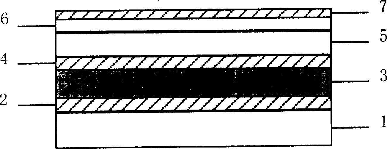
[0033] figure 1 It is a schematic diagram of the material structure of a quantum cascade semiconductor laser. Using molecular beam epitaxy (MBE) growth technology to grow a layer of N-type InGaAs lower waveguide layer 1 on the N-type InP substrate 1, and then grow 35 cycles of active regions 3 alternating InGaAs and InAlAs, and then grow N-type InGaAs The upper waveguide layer 4, because our solid-source MBE equipment does not have a P source, so after growing the waveguide core, the sample is cleaned with concentrated sulfuric acid, and then transferred to a metal-organic chemical vapor deposition (MOCVD) system to continue growing. layer N-type InP upper cladding layer 5, then grow N-type InP contact layer 6, and finally grow highly doped N-type InGaAs ohmic contact layer 7.

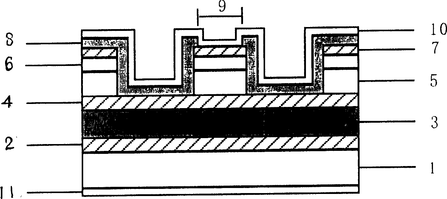
[0034] The device is a double-groove-ridge waveguide structure, and the epitaxial surface of the device is welded on the copper heat sink to further reduce the heat generation of the device. After th...


PUM


Abstract

A semiconductor laser cascaded by indium phosphide based quantum consists of a N type of indium phosphide substrate , a N type of indium gallium arsenide bottom wave guide layer ,an active region of indium gallium arsenide / indium aluminum arsenide alternitation in 35 cycles , a N type of indium gallium arsenide top wave guide layer , a N type of indium phosphide top clad layer , a N type of indium phosphide contact layer , a N type of indium gallium arsenide ohm contact layer , insulation layer on double channel mesa , a front N type of electrode and a back N type of electrode .

Description

technical field [0001] The invention relates to a device structure and a manufacturing method of a Fabry-Perot (F-P) cavity quantum cascade semiconductor laser, in particular to an indium phosphide-based quantum cascade semiconductor laser and a manufacturing method. Background technique [0002] Since the 3-5μm and 8-13μm mid-to-far infrared bands are very important atmospheric windows, lasers working in this band have very important application prospects in the fields of atmospheric environment detection, medical diagnosis, free space wireless optical communication, and infrared electronic countermeasures. However, the emission wavelength of conventional interband transition semiconductor lasers is limited by the forbidden band width of semiconductor materials, and it is very difficult to obtain semiconductor lasers with mid-to-far infrared or longer wavelengths. Therefore, scientists have carried out research on mid-to-far infrared quantum cascade semiconductor lasers bas...

Claims


Application Information

Patent Timeline
Patent Type & Authority Applications(China)
IPC IPC(8): H01S5/00
Inventor 郭瑜王春华刘俊岐刘峰奇王占国
Owner INST OF SEMICONDUCTORS - CHINESE ACAD OF SCI
Why Eureka
Try Eureka