Method for preparing focal plane of quantum trap infrared detecter

A technology of infrared detectors and quantum wells, applied in semiconductor devices, final product manufacturing, sustainable manufacturing/processing, etc., can solve problems such as indium column solder joint drop-off, lattice mismatch, thermal expansion coefficient mismatch, etc., to reduce Signal delay, no cross contamination, and reduced inductance

Inactive Publication Date: 2006-06-14
EAST CHINA NORMAL UNIVERSITY +1
View PDF0 Cites 19 Cited by
  • Summary
  • Abstract
  • Description
  • Claims
  • Application Information

AI Technical Summary

Problems solved by technology

[0004] 1. QWIP-ROIC adopts the method of direct upside-down interconnection or indirect upside-down interconnection method, under the action of repeated thermal cycle load of 300-30K cycles, the thermal expansion of the three materials of indium column, GaAs substrate of QWIP array and silicon-based ROIC Coefficient (CTE) mismatch, large stress changes cause viscoplastic deformat

Method used


Image

  • Method for preparing focal plane of quantum trap infrared detecter
  • Method for preparing focal plane of quantum trap infrared detecter
  • Method for preparing focal plane of quantum trap infrared detecter

Examples


Example Embodiment

[0039] The technical solution of the present invention will now be described in detail in conjunction with the accompanying drawings and embodiments. The embodiment is operated completely according to the above-mentioned operation steps.

[0040] Embodiment Preparation of Quantum Well Infrared Detector Focal Plane

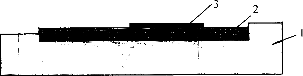
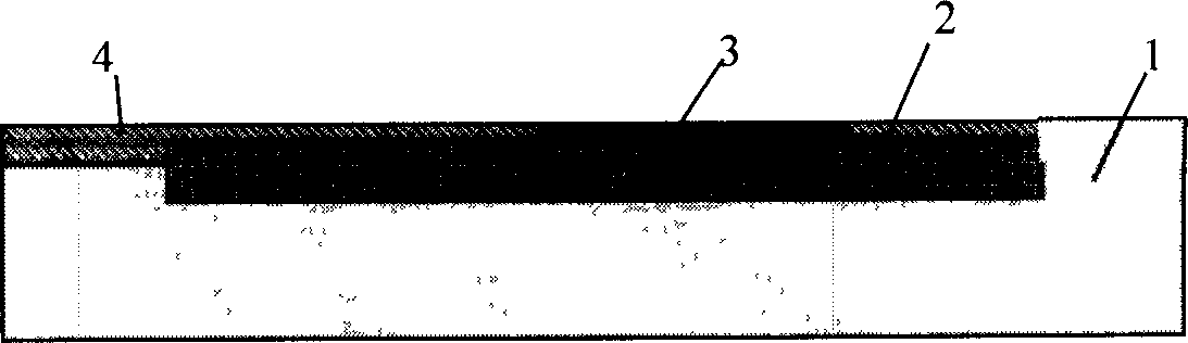
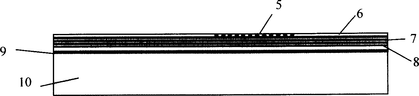
[0041] The preparation begins with two heterogeneous wafers. The diameter of the two heterogeneous wafers is 1 to 8 inches. The two heterogeneous wafers are respectively a silicon wafer 1 and a GaAs wafer 10, and a silicon-based readout integrated circuit 2 is formed on the silicon wafer 1. , GaAs wafer 10 is made with termination layer 9, lower electrode layer 8, quantum well layer 7, upper electrode layer 6 and two-dimensional grating 5, operation steps:

[0042] The first step is metal electrode processing of silicon-based readout integrated circuit 2

[0043] Evaporate CrAu or TiAu thin film 3 on silicon-based readout integrated circuit 2 by electron beam eva...


PUM

PropertyMeasurementUnit
Thicknessaaaaaaaaaa
Thicknessaaaaaaaaaa
Thicknessaaaaaaaaaa

Abstract

The invention is a method for preparing focal plane (FPA) of a quantum well infrared probe (QWIP), starting with two heterogeneous wafers, silicon wafer and GaAs wafer, where the silicon wafer and the GaAs wafer are made with a silicon-base read integrated circuit, and terminating layer, lower electrode layer, quantum well layer, upper electrode layer, and 2D grating, respectively; firstly using the chemical-mechanical flattening process to make the surface of the silicon wafer smooth, flat and clean and then aligning the upper electrodes of the smooth, flat and clean GaAs wafer with the corresponding metallic electrodes on the silicon wafer, using low-temperature heterogeneous wafer bonding method to bond the two wafers and make low-temperature thermal treatment until they are bonded together, then thinning the substrate of the GaAs wafer, selectively eating off the residual substrate, using corrosive solution to eat off the terminating layer, and finally completing the connection between the QWIP and the corresponding electrodes of the silicon-base read integrated circuit to obtain the productí¬FPA of QWIP. The method has the advantages of low cost, strong mechanical strength and good reliability.

Description

technical field [0001] The invention relates to a preparation method of a focal plane (FPA) of a quantum well infrared detector (QWIP). To be precise, it relates to a method for preparing QWIP-FPA by direct low-temperature heterogeneous bonding of QWIP and silicon-based readout integrated circuit (ROIC). It belongs to the field of optoelectronic integration technology. Background technique [0002] Due to the application of quantum well infrared detector (QWIP) focal plane (FPA) technology in meteorology, astronomy, earth observation, night vision, navigation, aircraft control, early warning system and other commercial, industrial and military fields, large-scale QWIP-FPA demand is growing. However, a large-scale QWIP-FPA is a complete FPA device formed by a large-scale QWIP photosensitive element array and a silicon-based readout signal integrated circuit, which are directly or indirectly interconnected through indium pillars grown separately. Th...

Claims


Application Information

Patent Timeline
IPC IPC(8): H01L31/18
CPCY02P70/50
Inventor 郭方敏甄红楼陆卫李宁林剑锋朱自强徐向晏忻佩胜陈效双郭少令赖宗声
Owner EAST CHINA NORMAL UNIVERSITY
Why Eureka
Try Eureka