Anisotropic conductive connector and wafer inspection device
An anisotropic and conductive technology, applied in the field of wafer inspection devices, can solve the problem of long distance of signal transmission system, and achieve the effect of maintaining stability, high conductivity and reducing size
- Summary
- Abstract
- Description
- Claims
- Application Information
AI Technical Summary
Problems solved by technology
Method used
Image
Examples
manufacture example 1
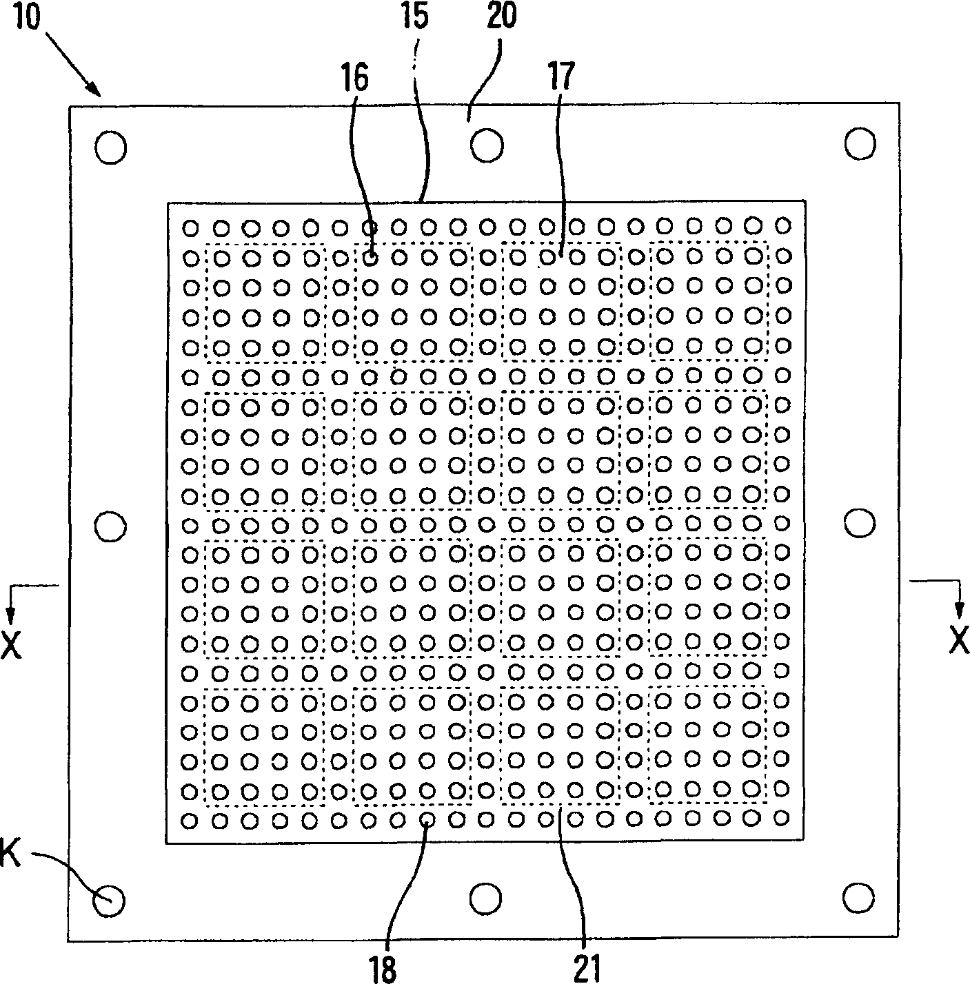
[0252] Prepare a brass plate with a thickness of 3.0mm, and drill holes in the X-X direction on one side of the non-magnetic material substrate (indicating the same as figure 1 The direction corresponding to the X-X direction shown. The same below) and the Y-Y direction (representing the direction perpendicular to the X-X direction. The same below) form a plurality of circular recesses with a diameter of 0.3mm and a depth of 2.7mm for accommodating magnetic components at a pitch of 0.8mm, and at the same time On the other side of the non-magnetic material substrate in the X-X direction and Y-Y direction, a plurality of recesses for forming protrusions with a diameter of 0.3 mm and a depth of 0.05 mm and a circular cross section are formed at a pitch of 0.8 mm. Substrate of non-magnetic material. In each magnetic member accommodation recess of the non-magnetic material substrate, a spherical magnetic member with a diameter of 0.3 mm made of iron is provided, and a cylindrical...
manufacture example 2
[0255] Prepare an iron plate with a thickness of 6mm, and use dry film photoresist and ferric chloride to perform photolithography on one side of the iron plate, so that the X-X direction on the ferromagnetic material substrate with a thickness of 5.9mm and made of iron Form a plurality of disc-shaped ferromagnetic material layers with a thickness of 0.1 mm and a diameter of 0.25 mm at a pitch of 0.65 mm in the Y-Y direction to form an intermediate body.
[0256] On one side of the intermediate body, on the region other than the ferromagnetic material layer, a non-magnetic material layer with a thickness of 0.15 mm is formed using a photoresist, thereby making an upper mold, and simultaneously making a lower mold in the same way. made Figure 7 Die for the structure shown. This mold is called "die b".
manufacture example 3
[0258] Prepare an iron plate with a thickness of 6mm, and use dry film photoresist and ferric chloride to perform photolithography on one side of the iron plate, so that the X-X direction on the ferromagnetic material substrate with a thickness of 5.9mm and made of iron A plurality of disc-shaped ferromagnetic material layers with a thickness of 0.1 mm and a diameter of 0.40 mm are formed at a pitch of 1.00 mm in the Y-Y direction to form an intermediate body.
[0259] On one side of the intermediate body, on the area other than the ferromagnetic material layer, a non-magnetic material layer with a thickness of 0.2 mm is formed using a photoresist, thereby making an upper mold, and at the same time making a lower mold by the same method, This makes Figure 7 Die for the structure shown. This mold is called "die c".
PUM
 Abstract
Description
Claims
Application Information


